Magnetic tunneling junction film structure with process determined in-plane magnetic anisotropy

a tunnel junction and film structure technology, applied in the direction of inductance/transformer/magnet manufacturing, magnetic bodies, instruments, etc., can solve the problems of non-planar surfaces, significant problems, and undesirable mtj devices having excessive magnetic coupling between adjacent magnetic layers, so as to prevent inadvertent switching of adjacent mtj cells, reduce coercivity, and improve shielding

Active Publication Date: 2005-07-21
HEADWAY TECH INC
View PDF17 Cites 47 Cited by
  • Summary
  • Abstract
  • Description
  • Claims
  • Application Information

AI Technical Summary

Benefits of technology

[0007] Some degree of anisotropy is necessary if an MTJ cell is to be capable of maintaining a magnetization direction and, thereby, to effectively store data even when write currents are zero. As cell sizes have continued to decrease, the technology has sought to provide a degree of magnetic anisotropy by forming cells in a wide variety of shapes (eg. rectangles, diamonds, ellipses, etc.), so that the lack of inherent crystalline anisotropy is countered by a shape anisotropy. Yet this form of anisotropy brings with it its own problems. A particularly troublesome shape-related problem in MTJ devices results from non-uniform and uncontrollable edge-fields produced by shape-anisotropy (a property of non-circular samples). As the cell size decreases, these edge fields become relatively more important than the magnetization of the body of the cell and have an adverse effect on the storage and reading of data. Although such shape anisotropies, when of sufficient magnitude, reduce the disadvantageous effects of super-paramagnetism, they have the negative effect of requiring high currents to change the magnetization direction of the MTJ for the purpose of storing data. To counteract these edge effects, Shi et al. (U.S. Pat. No. 5,757,695) teaches the formation of an ellipsoidal MTJ cell wherein the magnetization vectors are aligned along the length (major axis) of the cell and which do not present variously oriented edge domains, high fields and poles at the ends of the element. In addition, the fabrication processes required to produce the shape varieties, eg. photolithography and ion-milling, are incapable of controlling the shaping with sufficient precision to prevent variations in cell sizes, shapes and aspect ratios and, in addition, cause uncontrollable defects along the edges of the cells. The randomness of all these defects lead to a wide distribution in switching field coercivities (the fields required to change the logic state of an MTJ cell) and can even cause unwanted and uncontrollable coupling between cells. One attempt to reduce edge effects is provided by Nakao et al. (U.S. Pat. No. 6,351,410 B1), who form ring shaped MTJ electrodes to cause the induced magnetic fields to be circumferential.
[0008] As has been discussed, many of the problems associated with the construction of MRAM arrays are related to the shapes of the cells and the processes required to form those shapes. Cell shapes of present designs are typically single element rectangle, elliptical or lozenge. Any irregularities of these shapes, or defects at their edges produced during their formation, will result in coercivity fluctuations distributed throughout the array. An alternative approach to providing magnetic anisotropies without the necessity of utilizing shapes which are difficult to fabricate, is to produce a magnetic anisotropy in a ferromagnetic layer by forming it on an antiferromagnetic layer. In this way, a magnetic coupling can be produced between the ferromagnetic and antiferromagnetic layers which will provide the required magnetic anisotropy. In “Orientational dependence of the exchange biasing in molecular-beam-epitaxy-grown Ni80Fe20 / Fe50Mn50 bilayers” (R. Jungblut, R. Coehoorn, M. T. Johnson, J. aan de Stegge and A. Reinders, J. Appl. Phys. 75(10), 15 May 1994, pp. 6659-6664), experimental results are provided to show that interfacial exchange energy between such layers can be utilized to provide a biasing effect which lowers coercivity (as indicated by hysteresis loop shifts) in crystal growth directions. Fujikata et al. (U.S. Pat. No. 5,766,743) provide a magnetoresistance effect film having two ferromagnetic layers separated by a non-magnetic layer wherein one of the ferromagnetic layers is formed on an antiferromagnetic layer. The antiferromagnetic layer is at least partly made of a NiMn alloy having a face-centered tetragonal structure and it provides a biasing magnetic field, Hr, which exceeds the coercive force, Hc2, of the other ferromagnetic layer. The purpose of the antiferromagnetic layer is to provide domain stabilization of the free layer and, as a result the antiferromagnetic layer is not formed over the active region of the free layer. In a related invention, Rizzo et al. (U.S. Pat. No. 6,430,084 B1) teach the formation of bit and digit lines (the lines whose currents write and read the MTJ devices) which are clad with shielding ferromagnetic and antiferromagnetic layers to prevent inadvertent switching of adjacent MTJ cells. In the structure provided by Rizzo, the antiferromagnetic layer stabilizes the magnetization of the ferromagnetic layer by exchange coupling and thereby improves the shielding effect. It is the object of the present invention to utilize the magnetic coupling properties of antiferromagnetic layers with ferromagnetic layers to provide the necessary magnetic anisotropy to form an MTJ memory cell capable of advantageously storing data without the necessity of obtaining the anisotropy through the route of shape anisotropy. SUMMARY OF THE INVENTION
[0009] A first object of this invention is to provide a novel MTJ device whose magnetization switching properties are insensitive to shape irregularities and edge defects and which can be used to form an MRAM array.
[0010] A second object of this invention is to provide an MRAM array of such MTJ devices, in which array coercivity variations and resulting switching field variations due to shape irregularities and edge defects in the MTJ devices is eliminated or greatly reduced.
[0011] A third object of this invention is to provide an MRAM cell array design which is less dependent on the shape of individual cell elements for its performance.
[0012] A fourth object of this invention is to provide an MTJ cell which can be formed with a substantially circular shape of sub-micron dimension using even square shaped masks for cell patterning.

Problems solved by technology

Parkin also notes that such small sizes are associated with significant problems, particularly super-paramagnetism, which is the spontaneous thermal fluctuation of magnetization in samples of ferromagnetic material too small to have sufficient magnetic anisotropy (a measure of the ability of a sample to maintain a given magnetization direction).
It is also undesirable for MTJ devices to have excessive magnetic coupling between adjacent magnetic layers of neighboring devices or even within the same device as this coupling must be overcome when writing on the device.
One source of such undesirable coupling results from the non-planar surfaces at the interfaces of ferromagnetic layers, such as might occur between the fixed and free layer of an MTJ.
Yet this form of anisotropy brings with it its own problems.
A particularly troublesome shape-related problem in MTJ devices results from non-uniform and uncontrollable edge-fields produced by shape-anisotropy (a property of non-circular samples).
As the cell size decreases, these edge fields become relatively more important than the magnetization of the body of the cell and have an adverse effect on the storage and reading of data.
Although such shape anisotropies, when of sufficient magnitude, reduce the disadvantageous effects of super-paramagnetism, they have the negative effect of requiring high currents to change the magnetization direction of the MTJ for the purpose of storing data.
In addition, the fabrication processes required to produce the shape varieties, eg. photolithography and ion-milling, are incapable of controlling the shaping with sufficient precision to prevent variations in cell sizes, shapes and aspect ratios and, in addition, cause uncontrollable defects along the edges of the cells.
The randomness of all these defects lead to a wide distribution in switching field coercivities (the fields required to change the logic state of an MTJ cell) and can even cause unwanted and uncontrollable coupling between cells.
As has been discussed, many of the problems associated with the construction of MRAM arrays are related to the shapes of the cells and the processes required to form those shapes.
Any irregularities of these shapes, or defects at their edges produced during their formation, will result in coercivity fluctuations distributed throughout the array.

Method used


Image

  • Magnetic tunneling junction film structure with process determined in-plane magnetic anisotropy
  • Magnetic tunneling junction film structure with process determined in-plane magnetic anisotropy

Examples


Embodiment Construction

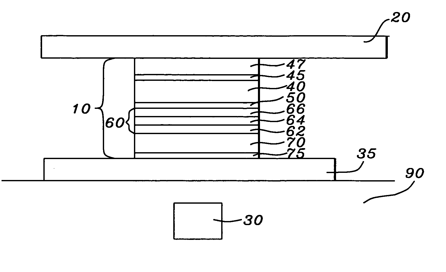
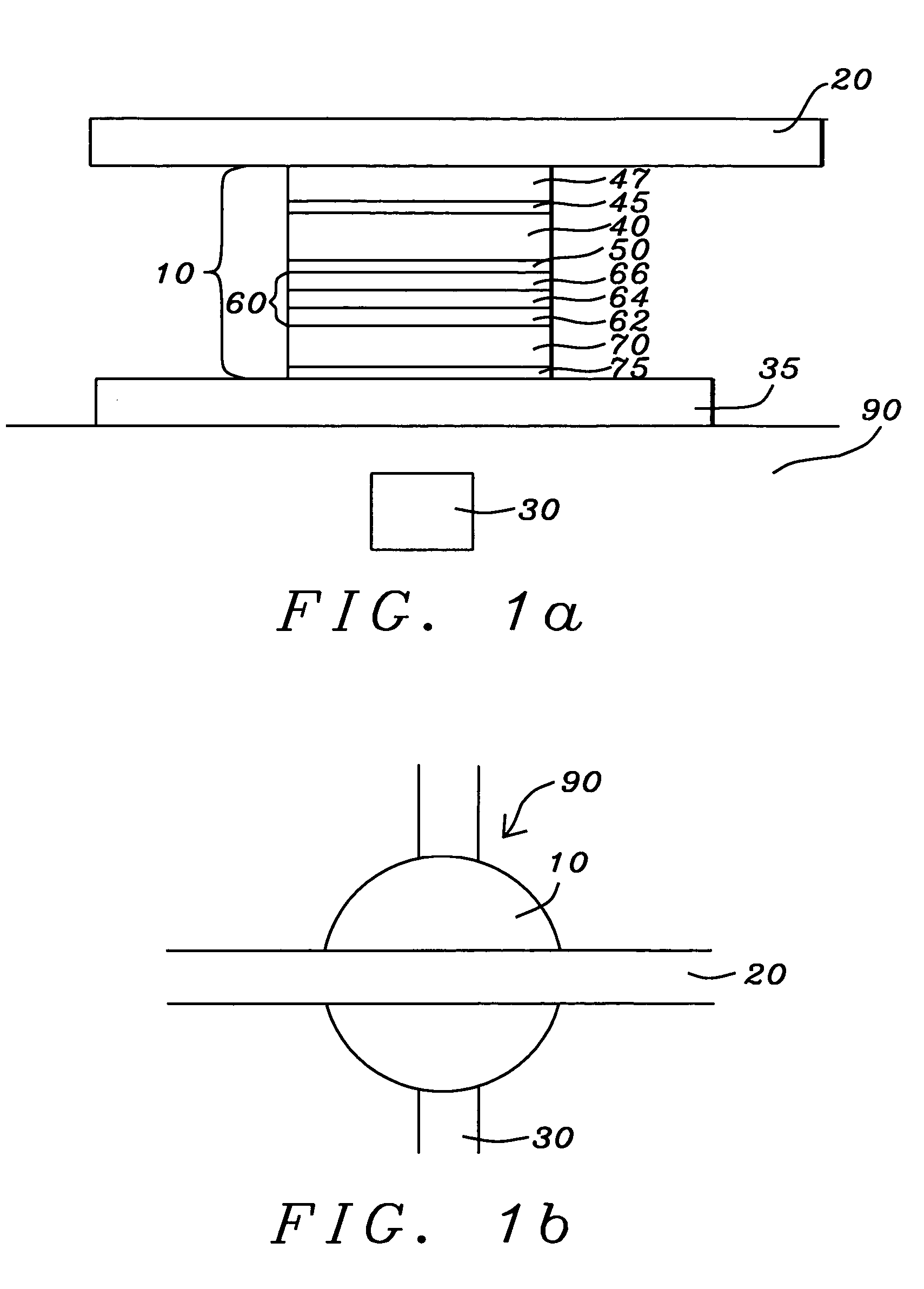
[0016] The preferred embodiment of the present invention teaches a method of forming an MTJ device (also called an MTJ memory cell) as one of an MRAM cell array of such devices, the ferromagnetic free layer of each such device having a magnetic anisotropy created by magnetic coupling through their interface with an antiferromagnetic layer.

[0017] Referring to FIG. 1a, there is shown a schematic vertical cross-sectional view of an MTJ cell (10) formed in accord with the method of the present invention. The cell is disposed between a substantially planar substrate, which contains a word line (30) that is insulated (90) from the cell and a bit line (20), which contacts an upper portion of the cell and which runs orthogonally to the word line. A lower conducting electrode (35) contacts a lower portion of the cell and is required for reading operations. The cell is thereby positioned at an orthogonal junction between the word and bit lines and is disposed between them. An overhead view o...


PUM


Abstract

A method of forming an MTJ memory cell and / or an array of such cells is provided wherein each such cell has a small circular horizontal cross-section of 1.0 microns or less in diameter and wherein the ferromagnetic free layer of each such cell has a magnetic anisotropy produced by a magnetic coupling with a thin antiferromagnetic layer that is formed on the free layer. The MTJ memory cell so provided is far less sensitive to shape irregularities and edge defects than cells of the prior art.

Description

BACKGROUND OF THE INVENTION [0001] 1. Field of the Invention [0002] This invention relates to the design and fabrication of magnetic tunnel junctions (MTJ) as memory storage devices, particularly to a design wherein coercivity and anisotropy are decoupled from the cell shape of the junction and can be independently optimized. [0003] 2. Description of the Related Art [0004] The magnetic tunnel junction (MTJ) basically comprises two electrodes, which are layers of ferromagnetic material, separated by a tunnel barrier layer, which is a thin layer of insulating material. The tunnel barrier layer must be sufficiently thin so that there is a probability for charge carriers (typically electrons) to cross the layer by means of quantum mechanical tunneling. The tunneling probability is spin dependent, however, depending on the availability of tunneling states with different electron spin orientations. Thus, the overall tunneling current will depend on the number of spin-up vs. spin-down elec...

Claims


Application Information

Patent Timeline
Patent Type & Authority Applications(United States)
IPC IPC(8): G11C11/14G11C11/16H01L27/105H01L21/8246H01L27/22H01L31/062H01L43/08H01L43/10H01L43/12
CPCB82Y25/00B82Y40/00G11C11/16H01L43/12H01F10/3272H01F41/307H01L43/08H01F10/3218G11C11/161H10N50/10H10N50/01
Inventor MIN, TAIHORNG, CHENGWANG, PO KANG
Owner HEADWAY TECH INC
Why Eureka
Try Eureka