Method and apparatus for an integrated laser beam scanner using a carrier substrate

a laser beam scanner and carrier substrate technology, applied in the direction of instruments, optical elements, electromagnetic radiation sensing, etc., can solve the problem that current techniques do not allow wafer-scale integration of light-emitter and mems devices, and achieve the effects of reducing complexity, improving functionality, and simplifying printing systems

Inactive Publication Date: 2004-02-24
XEROX CORP
View PDF12 Cites 18 Cited by
  • Summary
  • Abstract
  • Description
  • Claims
  • Application Information

AI Technical Summary

Benefits of technology

The present invention relates generally to the field of laser beam scanning systems, and more particularly to micro-electro-mechanical systems (MEMS) for laser beam scanning. Miniature laser beam scanning systems are important for applications such as barcode scanning, machine vision and, most importantly, xerographic printing. The use of MEMS to replace standard raster output scanning (ROS) in xerographic print engines allows s

Problems solved by technology

However, current techniques do not allow for wafer-sc

Method used


Image

  • Method and apparatus for an integrated laser beam scanner using a carrier substrate
  • Method and apparatus for an integrated laser beam scanner using a carrier substrate
  • Method and apparatus for an integrated laser beam scanner using a carrier substrate

Examples


Embodiment Construction

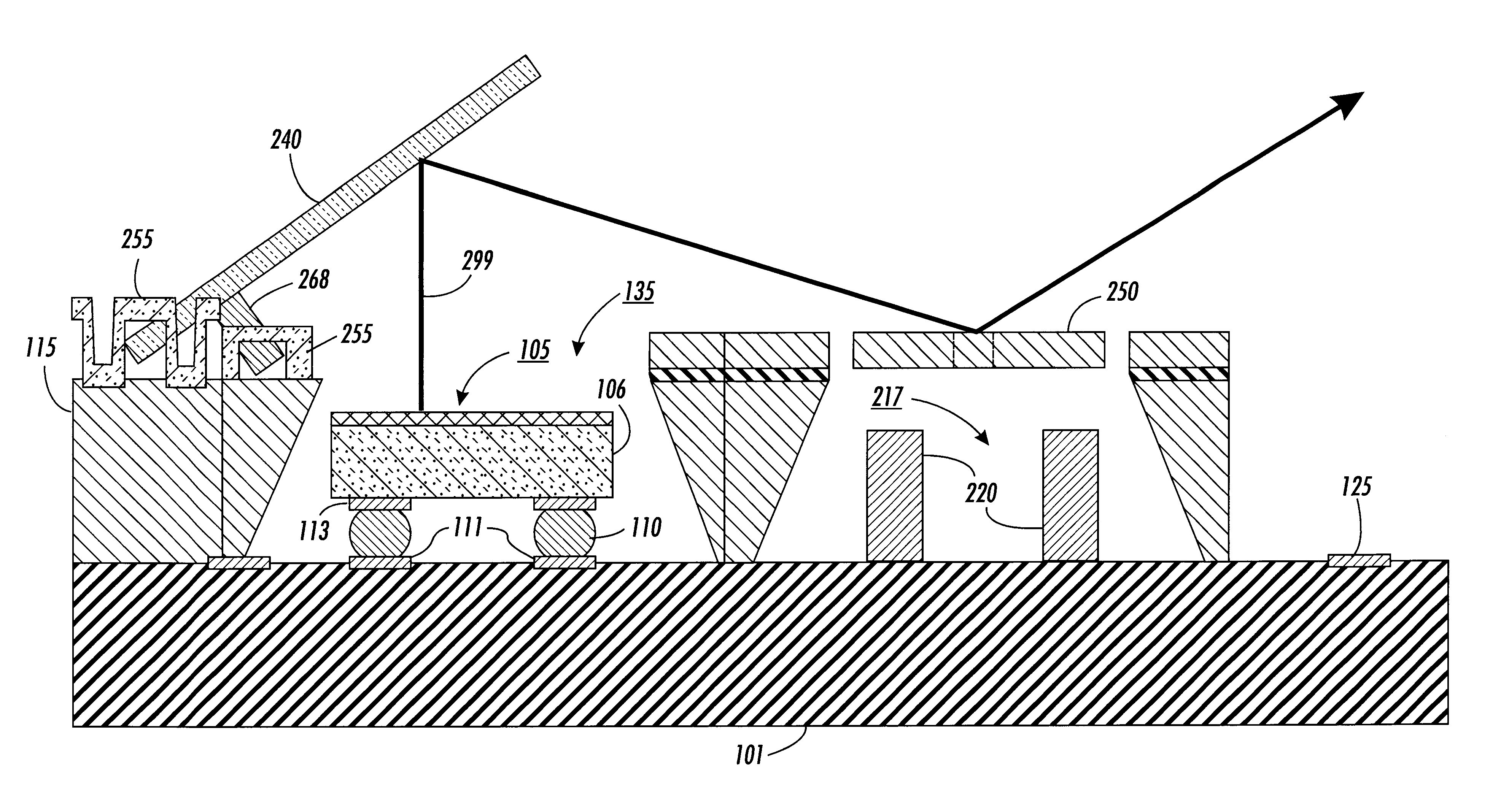
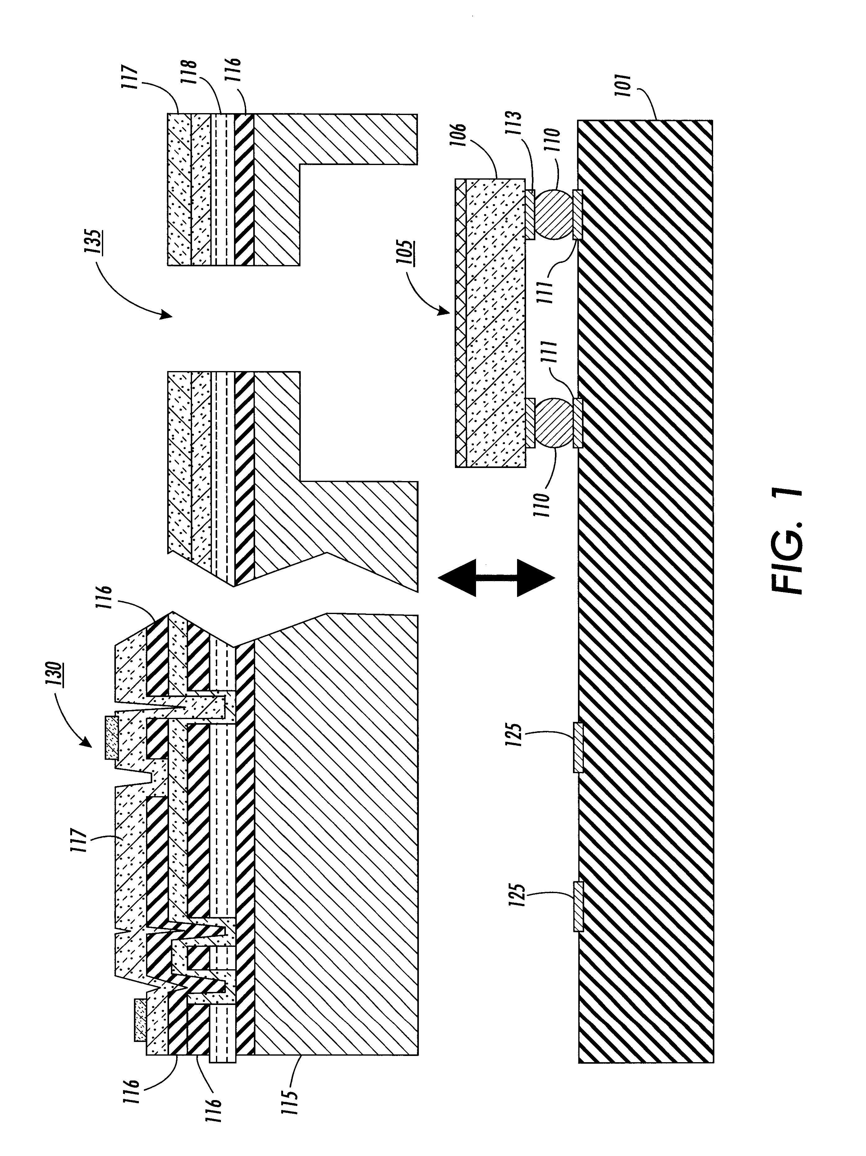
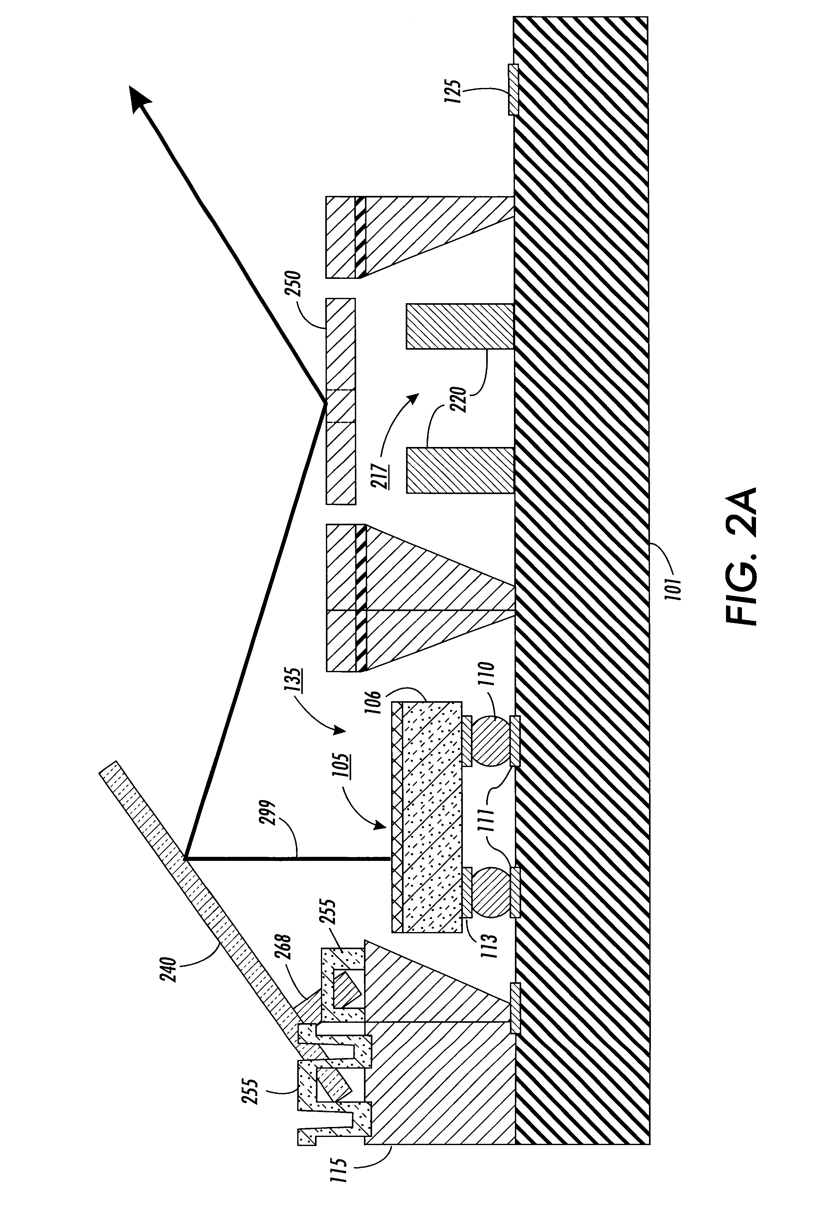
An embodiment in accordance with the present invention is shown in FIG. 1 and FIG. 2a. A laser beam scanner consisting of single crystal silicon (SCS) deflecting mirror 240 and torsional mirror 250 is integrated with laser diode or light emitting diode 105. Using solder bump bonding methods, completed and tested laser diodes 105 are bonded to glass or silicon carrier substrate 101. Carrier substrate 101 is aligned and bonded to MEMS substrate 130 containing the MEMS layers. Bonding of laser diode 105 to carrier substrate 101 completely partitions the bonding process from the MEMS layers. This complete partition eliminates possible conflicts between the conditions needed for solder bump bonding, such as the use of solder flux, and preserves the integrity of the MEMS layers. Typically, solders such as Pb / Sn, Au / Sn, or In / Sn are evaporated selectively onto wettable metal bonding pads 111 onto substrate 101 and reflowed to form hemispherical solder bumps 110. Solder bumps 110 are contac...


PUM


Abstract

An solid state scanning system having a single crystal silicon deflection mirror and scanning mirror is integrated with a light source. Separation of the micro-electro-mechanical systems and light emitters on separate substrates allows the use of flip-chip and solder bump bonding techniques for mounting of the light sources. The separate substrates are subsequently full wafer bonded together to create an integrated solid state scanning system.

Description

CROSS-REFERENCE TO RELATED APPLICATIONSThe present invention is related to "METHOD AND APPARATUS FOR AN INTEGRATED LASER BEAM SCANNER" by Floyd, Sun and Kubby (Attorney Docket No. D / 98706). Ser. No. 09 / 201738, filed on the same day and assigned to the same assignee which is hereby incorporated by reference in its entirety.BACKGROUND AND SUMMARY OF INVENTIONThe present invention relates generally to the field of laser beam scanning systems, and more particularly to micro-electro-mechanical systems (MEMS) for laser beam scanning. Miniature laser beam scanning systems are important for applications such as barcode scanning, machine vision and, most importantly, xerographic printing. The use of MEMS to replace standard raster output scanning (ROS) in xerographic print engines allows simplification of printing systems by eliminating macroscopic mechanical components and replacing them with large arrays of scanning elements. Advanced computation and control algorithms are used in managing...

Claims


Application Information

Patent Timeline
IPC IPC(8): G02B26/10G02B26/08G06K7/10
CPCG02B26/0833G02B26/0841G02B26/085G02B26/105G06K7/10653H01L2224/16225
Inventor FLOYD, PHILIP D.SUN, DECAIKUBBY, JOEL A.
Owner XEROX CORP
Why Eureka
Try Eureka