High speed method of aligning cutting lines of a workplace using patterns

Inactive Publication Date: 2006-03-21
KULICKE & SOFFA HLDG
View PDF6 Cites 28 Cited by
  • Summary
  • Abstract
  • Description
  • Claims
  • Application Information

AI Technical Summary

Benefits of technology

[0013]According to the present invention, the reference pattern at one point on the workpiece located at a preset position is registered in the storage means. Then, the patterns at two points in proximity to the center of the workpiece are imaged at the same time by the two imaging means which are provided at the pair of cutting blade units, and the control means drives the work mounting means so that the picked- up current image patterns at the two points can match with the reference pattern, thus aligning the workpiece. Next, either one of two imaging means is moved to a position to image a pattern at one point at the outer circumference of the workpiec

Problems solved by technology

Raising the cutting speed, however, may deteriorate the cutting performance, and raising the return speed excessively increases the vibrations of the dicing machine.
Thus, raising the cutting speed and the return speed does not achieve dramatic results, and therefore, the best way is raising the alignment speed.
The conventional wafer alignment method, however, has a problem in that the al

Method used


Image

  • High speed method of aligning cutting lines of a workplace using patterns
  • High speed method of aligning cutting lines of a workplace using patterns
  • High speed method of aligning cutting lines of a workplace using patterns

Examples


Embodiment Construction

[0022]This invention will be described in further detail by way of example with reference to the accompanying drawings with reference to the accompanying drawings.

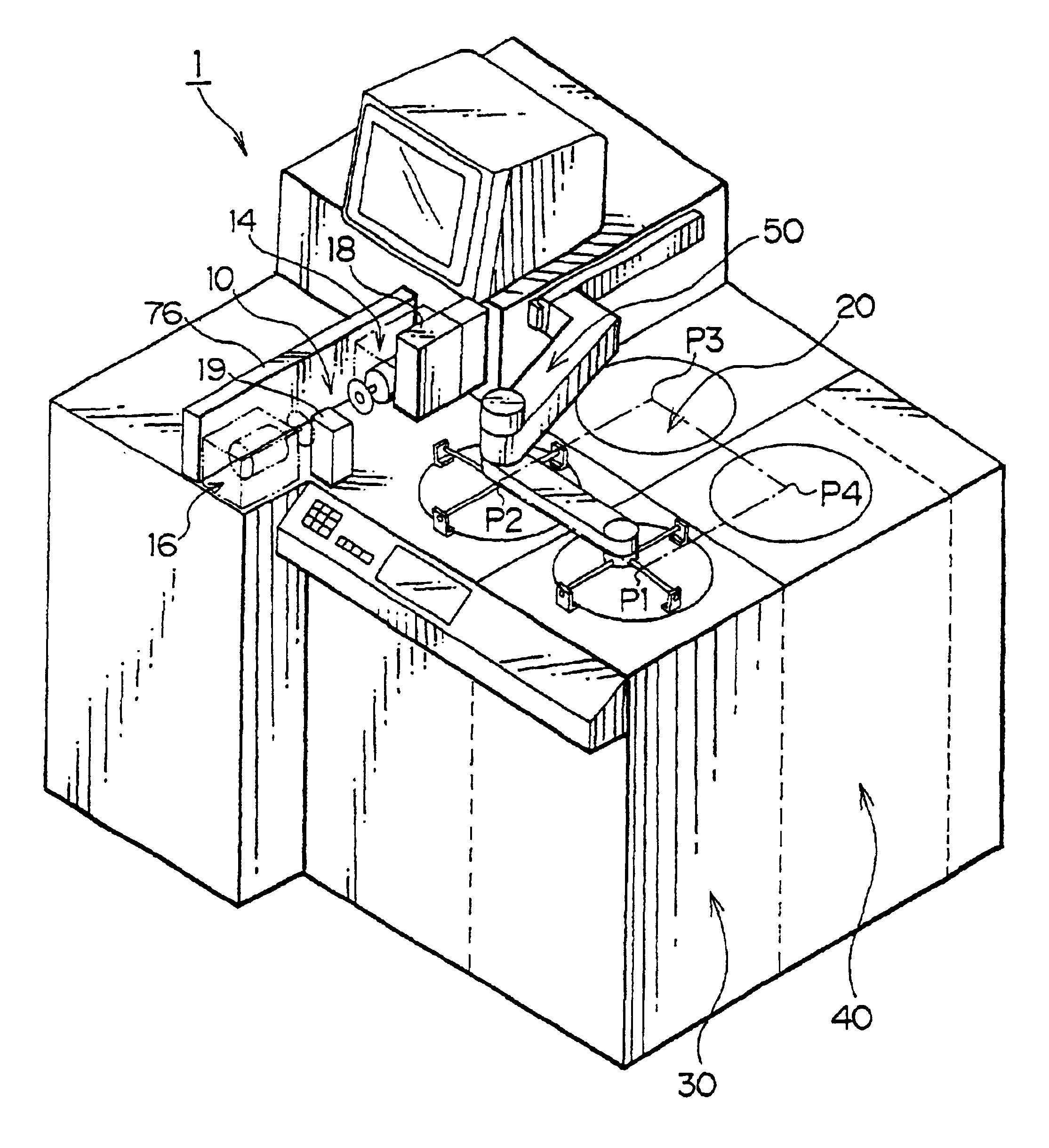
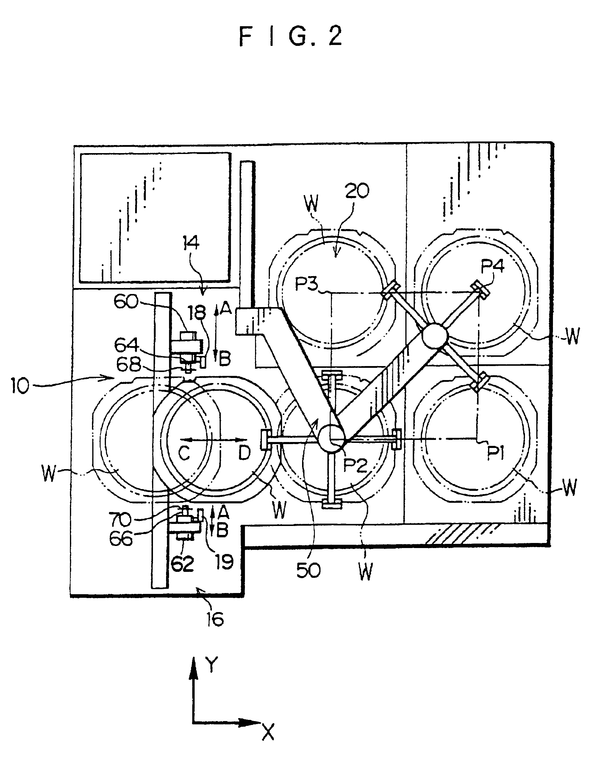
[0023]FIG. 1 is a perspective view of a dicing machine 1 for a semiconductor wafer according to the present invention, and FIG. 2 is a plan view of the dicing machine 1. As shown in FIG. 1, the dicing machine 1 is comprised mainly of a cutting part 10, a cleaning part 20, a cassette housing part 30, an elevator part 40 and transport equipment 50.

[0024]A description will be given of a cutting process of the dicing machine 1. First, a plurality of wafers W, which are housed in the cassette housing part 30, are sequentially retrieved by the elevator part 40, and the retrieved wafer W is set at a position P4 in FIG. 2. The wafer W is placed on a cutting table (position P2: see FIG. 4) 12 of the cutting part 10 via a pre-load stage at a position P1. The wafer W is vacuumed to the cutting table 12. Imaging equipment 18, 19 for a...


PUM

PropertyMeasurementUnit
Angleaaaaaaaaaa
Timeaaaaaaaaaa
Speedaaaaaaaaaa

Abstract

Two imaging equipment are provided at a pair of cutting blade units, and the two imaging equipment image patterns at first positions in proximity to the center of a wafer at the same time. A controller drives drive mechanisms to align the wafer in such a way that current image patterns at the first positions can match with a reference pattern at the first positions. Then, the two imaging equipment are moved to positions for imaging patterns at second positions at the outer circumference of the wafer to image the patterns at the second positions. The controller drives the drive mecha- nisms to align the wafer in such a way that current image patterns at the second positions can match with a reference pattern at the second positions.

Description

BACKGROUND OF THE INVENTION[0001]1. Field of the Invention[0002]The present invention relates generally to an alignment method and apparatus applied to a worktable of a semicon- ductor dicing machine, and more particularly to a wafer alignment method and apparatus of a dicing machine, which cuts a semiconductor wafer ( a workpiece) into squares with a pair of cutting blade units.[0003]2. Description of Related Art[0004]The processing speed of the dicing machine has become higher, whereas the diameter of the semiconductor wafer has become larger. To reduce the processing time, a cutting speed is raised, a return speed is raised, or an alignment speed is raised. Raising the cutting speed, however, may deteriorate the cutting performance, and raising the return speed excessively increases the vibrations of the dicing machine. Thus, raising the cutting speed and the return speed does not achieve dramatic results, and therefore, the best way is raising the alignment speed.[0005]FIG. 7 is...

Claims


Application Information

Patent Timeline
IPC IPC(8): B28D1/04B23D59/00H01L21/68B27B31/06B28D5/02H01L21/301
CPCB23D59/002B27B31/06B28D5/029Y10T83/6587Y10T83/7697
Inventor AZUMA, MASAYUKISHIMODA, HIROFUMIFISCHER, MANI
Owner KULICKE & SOFFA HLDG
Why Eureka
Try Eureka