Spacer-type thin-film polysilicon transistor for low-power memory devices

a technology of low-power memory and polysilicon, which is applied in the direction of transistors, semiconductor devices, electrical equipment, etc., can solve the problems of difficult manufacturing of devices using such geometries, the small polysilicon grain size of these layers is also very small, and the leakage of bitline to supply (vcc) is still too significant to enable battery operation of high-density memory devices, such as srams, over an extended period of time, so as to minimize the leakag

Inactive Publication Date: 2010-01-05
STMICROELECTRONICS SRL
View PDF23 Cites 0 Cited by
  • Summary
  • Abstract
  • Description
  • Claims
  • Application Information

AI Technical Summary

Benefits of technology

[0005]It would be advantageous in the art to minimize bitline to supply (Vcc) leakage of thin-film transistors (TFTs).
[0006]It would further be advantageous in the art to be able to reduce the cross-sectional area of a TFT channel in order to minimize bitline to supply (Vcc) leakage of a thin-film transistor (TFT).
[0007]Therefore, according to the present invention, the cross-sectional area of a thin-film transistor (TFT) is decreased in order to minimize bitline to supply leakage of the TFT. This is accomplished by utilizing a spacer etch process to manufacture a TFT having a very narrow and thin channel in a controllable manner. The spacer dimensions of the TFT may be adjusted by simply modifying the thicknesses of the poly gate and the channel poly. The channel thickness is limited by the thickness; of deposited channel polysilicon which may be as thin as approximately 300 Å to 500 Å, and the channel width of the TFT corresponds to the height of the spacer etched along the polysilicon gate of the device which may be as small as approximately 0.15 to 0.25 μm.
[0008]A first preferred embodiment of the present invention employs at least two polysilicon layers to effect a spacer etch process which allows the cross-sectional area of a transistor channel of a TFT to be minimized in a controllable manner, thereby reducing the bitline to voltage supply leakage of the TFT. The first preferred embodiment provides planarization as an option. A second preferred embodiment of the present invention also utilizes a spacer etch process by selective etching a poly spacer of a spacer-TFT load structure formed around a first poly gate layer in order to achieve the desired channel length. The second preferred embodiment offers the advantage of requiring just two polysilicon layers; planarization is not required.

Problems solved by technology

In spite of this advantage, however, the bitline to supply (Vcc) leakage of TFTs designed and fabricated in state-of-the-art technology is still too significant to enable battery operation of high-density memory devices, such as SRAMs, over an extended period of time.
Unfortunately, the resultant polysilicon grain size of these layers is also very small.
As would be anticipated, this difference between the width dimension and other CDs of the memory device places considerable pressure on the photolithography aspect of manufacturing and thus makes manufacturing of a device using such geometries very difficult.
This results in process complications which do not render a viable manufacturing approach.

Method used


Image

  • Spacer-type thin-film polysilicon transistor for low-power memory devices
  • Spacer-type thin-film polysilicon transistor for low-power memory devices
  • Spacer-type thin-film polysilicon transistor for low-power memory devices

Examples


first embodiment

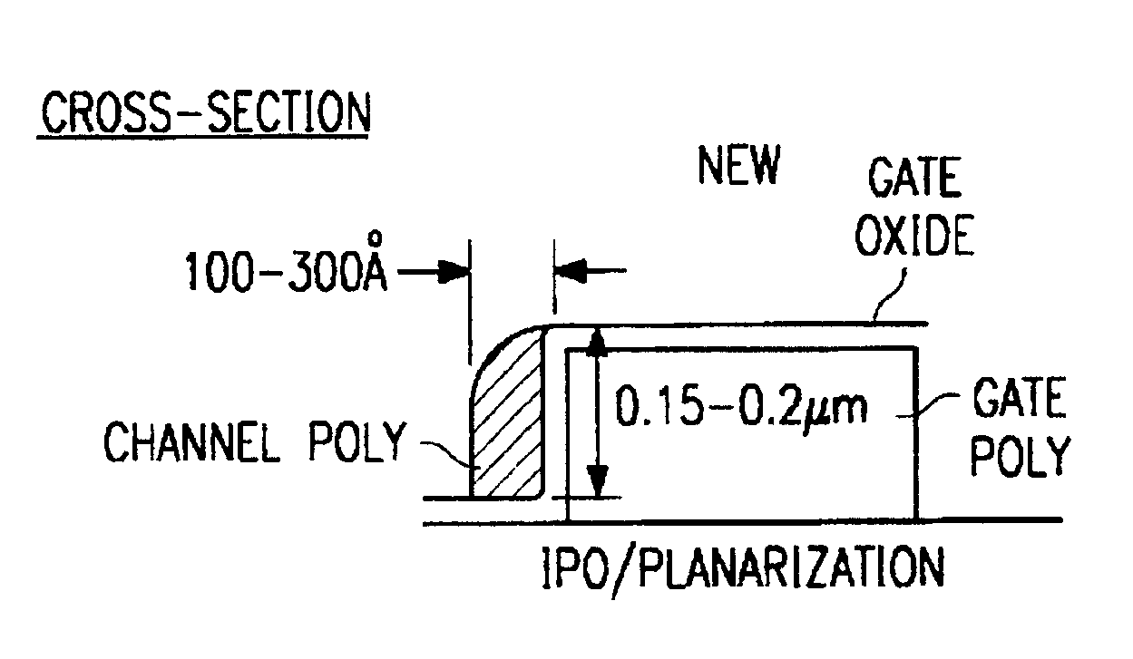
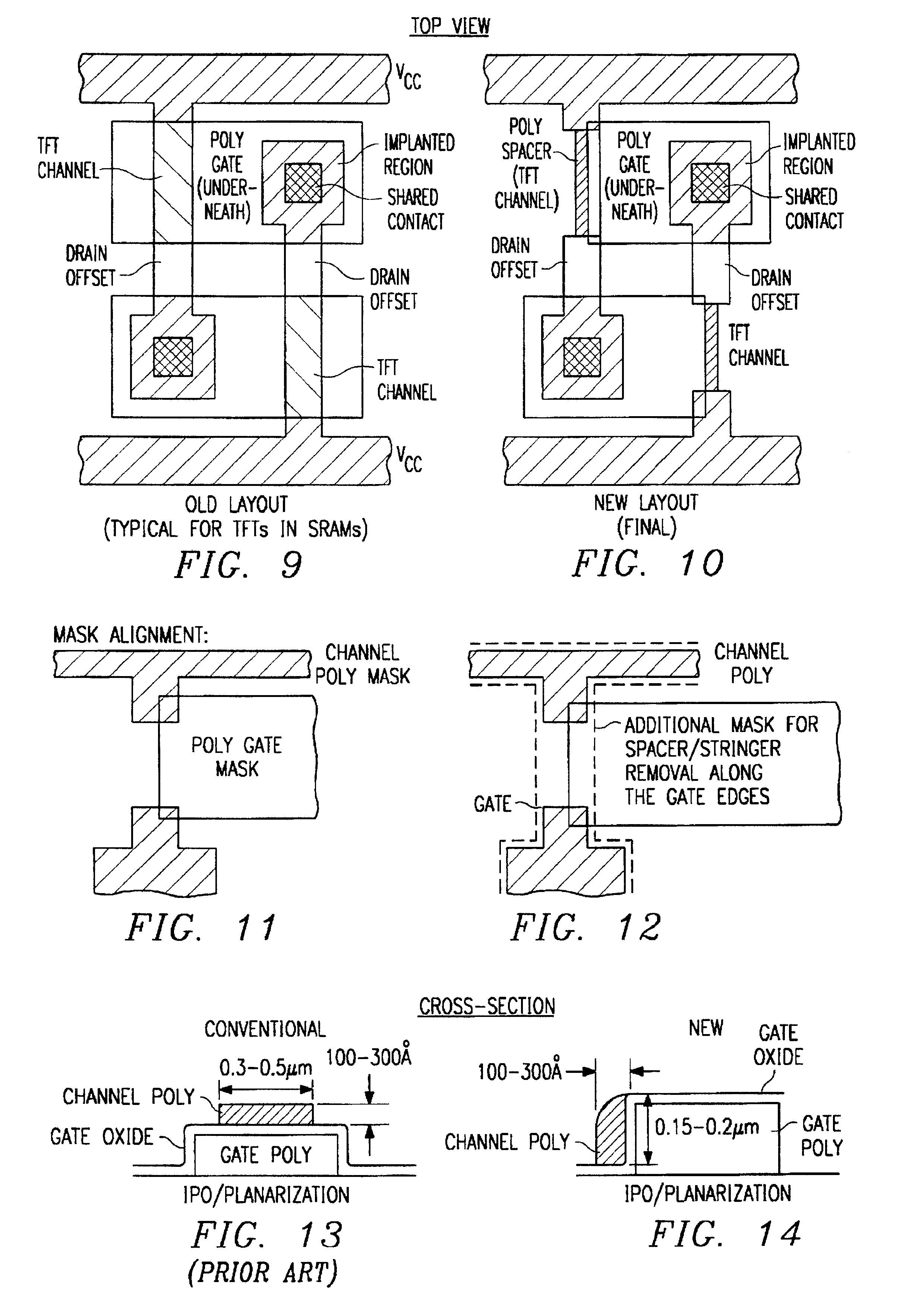
[0023]An understanding of the first preferred embodiment of the present invention is further aided by comparing the cross-sectional view of a conventional TFT structure of FIG. 13 with the cross-sectional view of the present invention shown in FIG. 14. The cross-sectional area of the conventional TFT channel is shown as approximately 0.3 to 0.5 μm by approximately 300 to 500 Å, requiring special lithography tools, as mentioned above. The cross-sectional area of the TFT channel of the present invention is much smaller and is approximately 0.15 to 0.2 μm approximately 300 to 500 Å. This is achieved without any lithography-related constraints.

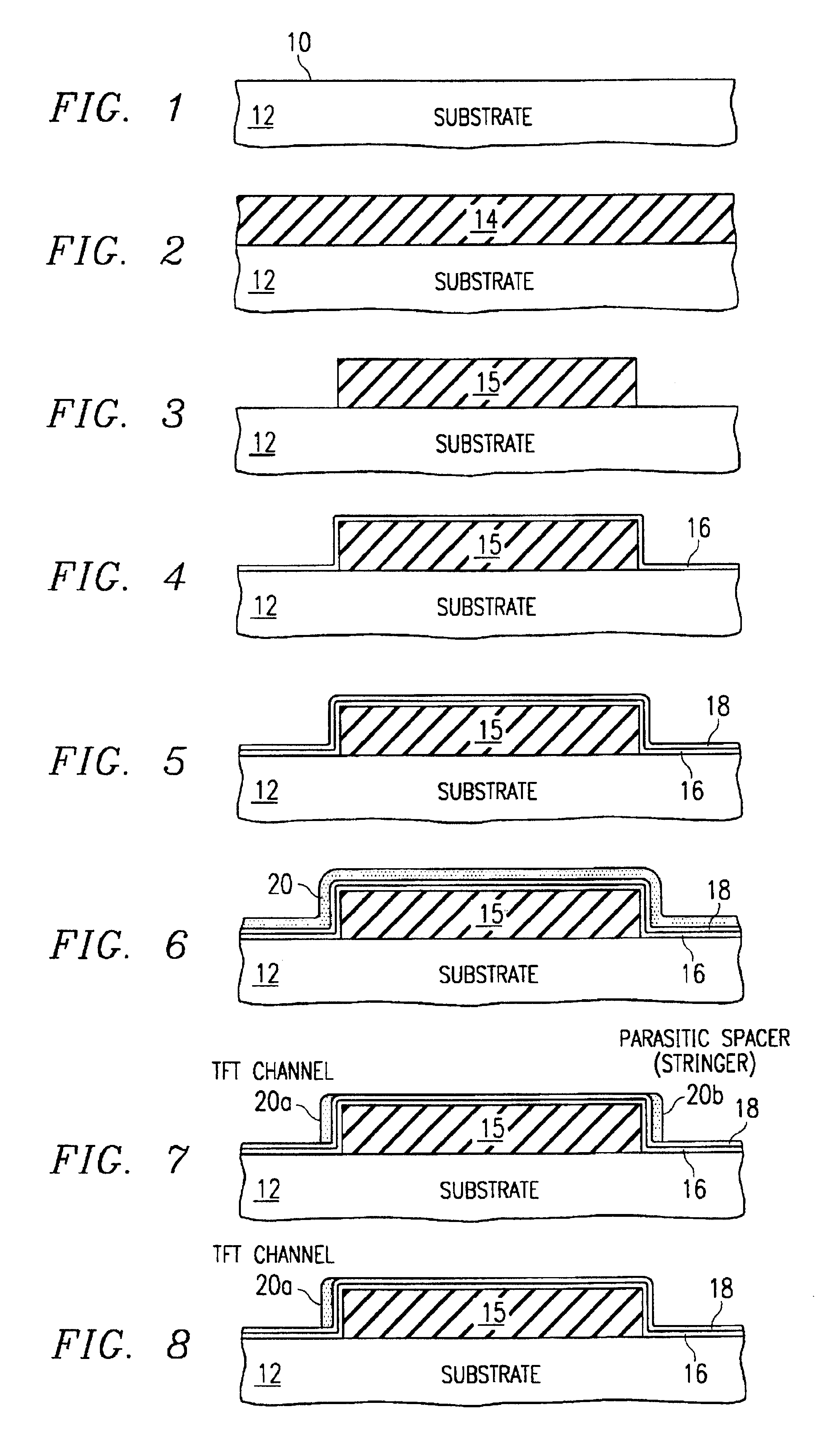
[0024]The process steps and structure of the first preferred embodiment of the present invention, represented in FIGS. 1-14, illustrate a TFT device having a channel that is both very narrow and thin. However, the first preferred embodiment of the present invention requires at least two poly layers: one or two poly layers formed in the standard pr...

second embodiment

[0032]In addition to utilizing only two poly layers rather than three poly layers and not requiring planarization, the present invention offers other desirable features. The simultaneously salicided Vss and Vcc voltage supply lines of the second preferred embodiment allow for reduced series resistance. Additionally the TFT source (P+) connected to the pull-down gate (N+) through the TaSi or WSi layer ensures that there is no problematic N+ / P+ parasitic junction.


PUM


Abstract

The cross-sectional area of a thin-film transistor (TFT) is decreased in order to minimize bitline to supply leakage of the TFT. This is accomplished by utilizing a spacer etch process to manufacture a TFT having a very narrow and thin channel in a controllable manner. The spacer dimensions of the TFT may be adjusted by simply modifying the thicknesses of the poly gate and the channel poly. The channel thickness is limited by the thickness of the deposited channel polysilicon which may be as thin as approximately 300 Å to 500 Å, and the channel width of the TFT corresponds to the height of the spacer etched along the polysilicon gate of the device which may be as small as approximately 0.15 to 0.25 μm.

Description

[0001]This application is a continuation application of U.S. patent application Ser. No. 09 / 334,877, filed Jun. 17, 1999, and is now abandoned, which is a reissue of U.S. patent application Ser. No. 08 / 521,709, filed Aug. 31, 1995, which is now U.S. Pat. No. 5,640,023, issued Jun. 17, 1997.BACKGROUND OF THE INVENTION[0002]The present invention relates generally to integrated circuit memory devices, and more specifically to integrated circuit memory devices which employ thin-film transistor (TFT) technology.[0003]Thin-film transistors (TFTs) are becoming the load devices of choice in many integrated circuit memory devices, particularly in static random access memory (SRAM) cells. TFTs are superior to standard polysilicon resistor load devices, in that TFTs have an inherently lower OFF current—an advantage which is particularly relevant in low—and zeropower SRAM applications which feature extended battery operation. In spite of this advantage, however, the bitline to supply (Vcc) leak...

Claims


Application Information

Patent Timeline
Patent Type & Authority Patents(United States)
IPC IPC(8): H01L29/76H01L31/036H01L21/336H01L21/8244H01L27/11H01L29/786
CPCH01L27/11H01L29/78696H01L27/1108H10B10/125H10B10/00
Inventor BALASINSKI, ARTUR P.HUANG, KUEI-WU
Owner STMICROELECTRONICS SRL
Why Eureka
Try Eureka