Boost clock generation circuit and semiconductor device

A clock generation circuit and clock technology, which is applied in the manufacturing of semiconductor devices, circuits, and semiconductor/solid-state devices, etc., can solve the problems of increasing and weakening the scale of the boost clock circuit, reducing the through current, reducing the current of charging and discharging, Avoid the effect of simultaneous conduction

Inactive Publication Date: 2007-12-19
SEIKO EPSON CORP
View PDF4 Cites 0 Cited by
  • Summary
  • Abstract
  • Description
  • Claims
  • Application Information

AI Technical Summary

Problems solved by technology

[0008] Moreover, even if the above-mentioned effect can be obtained, as the number of switching elements increases, the circuit scale for generating the boost clock will increase, and the effect of cost reduction will also be weakened. Therefore, it is necessary to use a simpler structure to generate The boost clock of the charge pump circuit that achieves the above effects

Method used


Image

  • Boost clock generation circuit and semiconductor device
  • Boost clock generation circuit and semiconductor device
  • Boost clock generation circuit and semiconductor device

Examples


Embodiment Construction

[0063] Preferred embodiments of the present invention will be described in detail below with reference to the accompanying drawings. The present embodiment described below does not unduly limit the content of the present invention described in the claims, and not all the configurations described in the present embodiment are necessarily adopted as solutions of the present invention.

[0064] First, a charge pump circuit suitable for inclusion in a semiconductor device (integrated circuit, IC) will be described. Next, a boost clock generating circuit suitable for generating the boost clock of the charge pump circuit will be described.

[0065] 1. Charge pump circuit

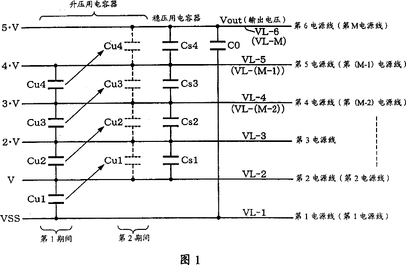
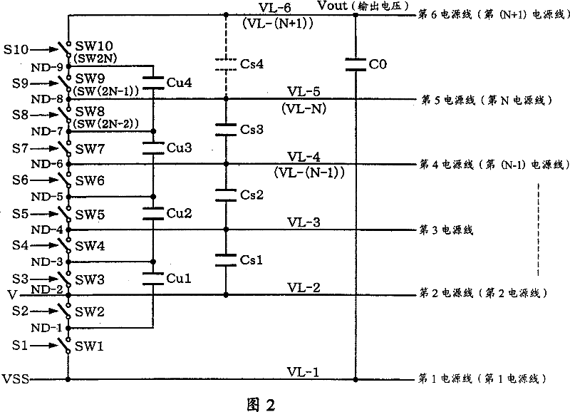
[0066] The boosted clock circuit of this embodiment includes at least two capacitors, that is, the boosted voltage is output by the charge pump method.

[0067] FIG. 1 shows an explanatory diagram of the working principle of the charge pump circuit of this embodiment. The charge pump circuit of this embodiment ...


PUM


Abstract

A boost clock generation circuit (500) including: a first switch circuit (502) connected between a first power supply line and a first clock output line to which the first boost clock signal is output; a second switch circuit (504) connected between a second power supply line and the first clock output line; a third switch circuit (506) connected between a third power supply line and a second clock output line to which the second boost clock signal is output; and a fourth switch circuit (508) connected between a fourth power supply line and the second clock output line. One of the first and second switch circuits is exclusively turned ON, and one of the third and fourth switch circuits is exclusively turned ON. The level of current drive capability of the first switch circuit differs from the level of current drive capability of the third switch circuit; and the level of current drive capability of the second switch circuit differs from the level of current drive capability of the fourth switch circuit.

Description

technical field [0001] The present invention relates to a boost clock generation circuit and a semiconductor device. Background technique [0002] As a display device, a liquid crystal display device having an electro-optical device is generally used. By assembling the liquid crystal display device in electronic equipment, the miniaturization of the electronic equipment and the reduction of current consumption can be achieved simultaneously. [0003] However, driving a liquid crystal display device requires a high voltage. Therefore, it is in line with the viewpoint of cost reduction to incorporate a power supply circuit that generates a high voltage in a driver IC (Integrated Circuit) (semiconductor device in a broad sense) that drives an electro-optical device. At this time, the power supply circuit has a booster circuit. The boost circuit boosts the voltage between the system power supply voltage VDD on the high potential side and the ground power supply voltage VSS on...

Claims


Application Information

Patent Timeline
Patent Type & Authority Patents(China)
IPC IPC(8): H02M3/07H01L27/00G09G3/20H01L21/822H01L27/04H03K17/06H03K19/096
CPCH02M3/07
Inventor 上条治雄
Owner SEIKO EPSON CORP
Why Eureka
Try Eureka