
Organic electroluminescence device

An electroluminescent device, an organic technology, applied in the direction of electroluminescent light source, electric light source, electrical components, etc., can solve the problems affecting the performance of the light-emitting layer, the complex energy band structure, and the performance of the device, so as to improve the transmission performance. Enhanced luminous efficiency and high binding energy effects

Inactive Publication Date: 2008-07-16
SUN YAT SEN UNIV
View PDF3 Cites 0 Cited by
  • Summary
  • Abstract
  • Description
  • Claims
  • Application Information

AI Technical Summary

Problems solved by technology

[0010] As we all know, most organic semiconductor materials are weak p-type, and their ability to conduct holes is several orders of magnitude higher than their ability to conduct electrons, while there are very few organic semiconductor materials with excellent electron conduction ability, which often leads to the light emission of OLEDs The hole concentration in the layer is higher than the electron concentration, causing recombination imbalance and affecting device efficiency
The (electronic) energy band structure of the interface between organic materials is very complex, and the interaction and mixing of organic materials at the interface will also cause trapping and quenching of carriers and excitons, which will affect device performance.
In addition, the shape change of the organic carrier transport material due to poor stability will affect the performance of the light-emitting layer, and seriously cause the entire device to fail.

Method used


Image

  • Organic electroluminescence device

Examples


Embodiment Construction

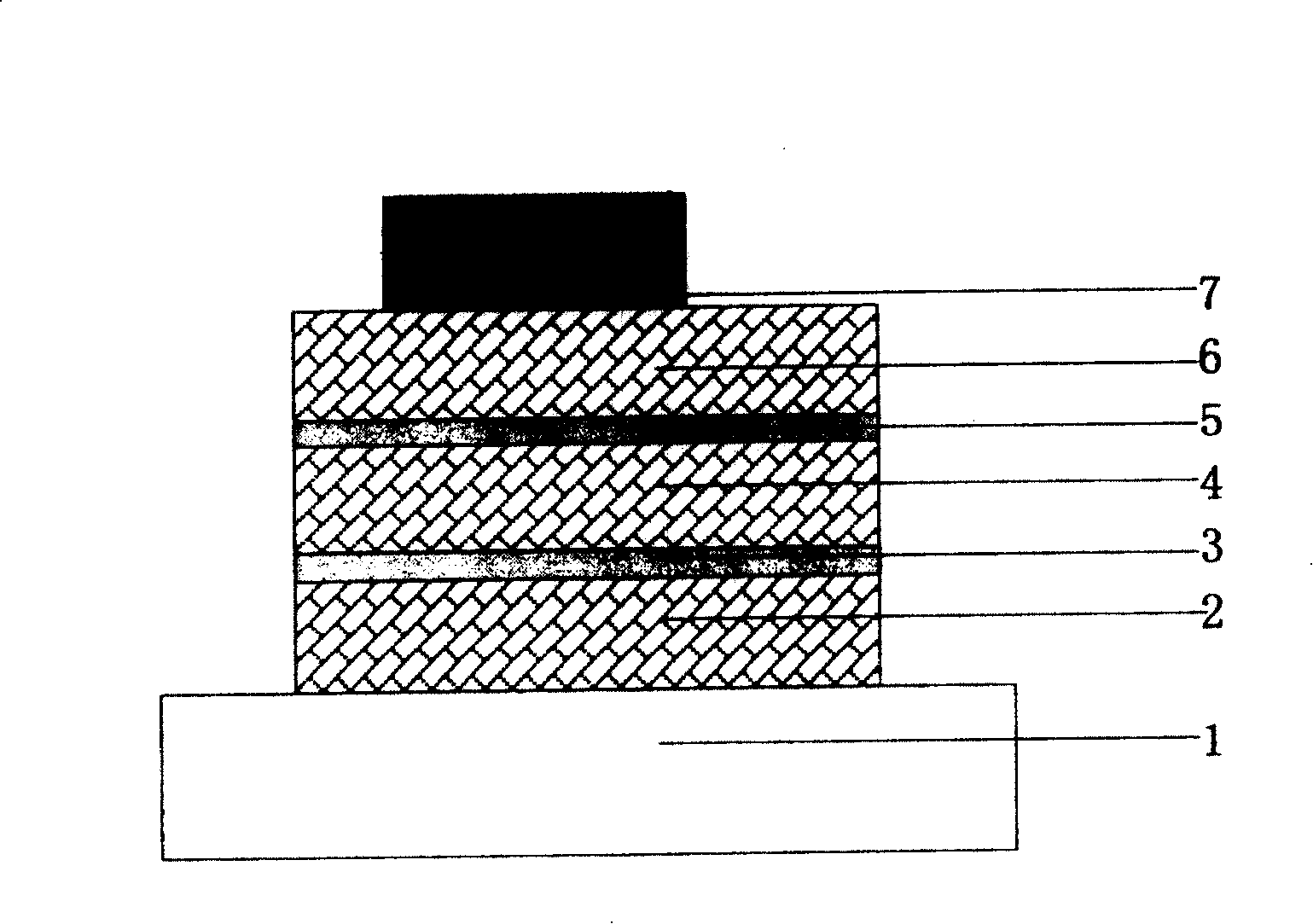
[0030]First, on the cleaned ITO conductive glass electrode (1) substrate, a layer of aromatic diamine derivative TPD with a thickness of 40nm is evaporated as a hole transport layer (2) by vacuum thermal evaporation coating method, and then evaporated on One deck thickness is the 8 quinoline aluminum Alq of 20nm as light-emitting layer (4), then vapor deposition last layer thickness is 0.5nm (device 1) or 1nm (device 2) thick LiF inorganic material thin layer ( 5) As a hole and exciton blocking layer, then vapor-deposited a layer of 8-hydroxyquinoline aluminum Alq with a thickness of 40nm as the electron transport layer (6), and finally vapor-deposited with a layer of metal aluminum Al with a thickness of 100nm as Back electrode (7). In the device, the inorganic material thin layer (3) may not be used, and the light emitting layer (4) and the electron transport layer (6) may be of the same material. Compared with the conventional devices prepared by the prior art under the sa...


PUM


Abstract

The organic electroluminescent device consists of: an ITO conducting glass electrode; an organic material holes transport layer; an inorganic material film; an organic material light emission layer; an inorganic material film; an organic electron transport layer; a metal reverse side electrode. The inorganic material film is used in the organic light emission layer and carrier transport layer to block off excess carrier, or to accelerate minority carrier transport and control excition transition, then to implement equilibrium of carrier and increase the light emission efficiency of the component. Through controlling the thickness and location of the inorganic material film, the electric field distribution, the carrier distribution, the excition distribution, the light color and light area can be adjusted.

Description

technical field [0001] The invention relates to an organic electroluminescence device, which belongs to the technical field of organic electroluminescence. Background technique [0002] Organic light-emitting diodes (Organic Light-emitting diodes, referred to as OLEDs), as a new, next-generation flat-panel display technology and light source, have both active light emission, wide viewing angle, full color, bendable, high efficiency, Many advantages such as low power consumption and low cost meet the requirements of display technology for the development trend of mobile communication and information display in the information age. Its broad application prospects and breakthroughs in materials and devices in recent years make it an extremely One of the competitive new flat panel display technologies and lighting technologies. [0003] The research on OLEDs technology originated in the 1960s, and the breakthroughs are mainly as follows: [0004] (1) In 1987, C.W.Tang and S.A....

Claims


Application Information

Patent Timeline
Patent Type & Authority Patents(China)
IPC IPC(8): H01L51/50H05B33/22H05B33/10
Inventor 周翔连加荣刘彭义曹玲芳许宁生
Owner SUN YAT SEN UNIV
Learn More