TFT LCD array substrate peripheral wiring structure and its producing method

A technology of array substrates and peripheral wiring, applied in semiconductor/solid-state device manufacturing, nonlinear optics, optics, etc., can solve problems such as large coupling effects, reduce overlapping areas, increase spatial distance, and reduce capacitive coupling effects Effect

Active Publication Date: 2008-10-01
BOE TECH GRP CO LTD +1
View PDF4 Cites 0 Cited by
  • Summary
  • Abstract
  • Description
  • Claims
  • Application Information

AI Technical Summary

Problems solved by technology

It can be seen from the figure that the repair line 1 and the peripheral common electrode line 2 have a large area of ​​overlap, so the coupling effect is correspondingly large

Method used


Image

  • TFT LCD array substrate peripheral wiring structure and its producing method
  • TFT LCD array substrate peripheral wiring structure and its producing method
  • TFT LCD array substrate peripheral wiring structure and its producing method

Examples


Embodiment 1

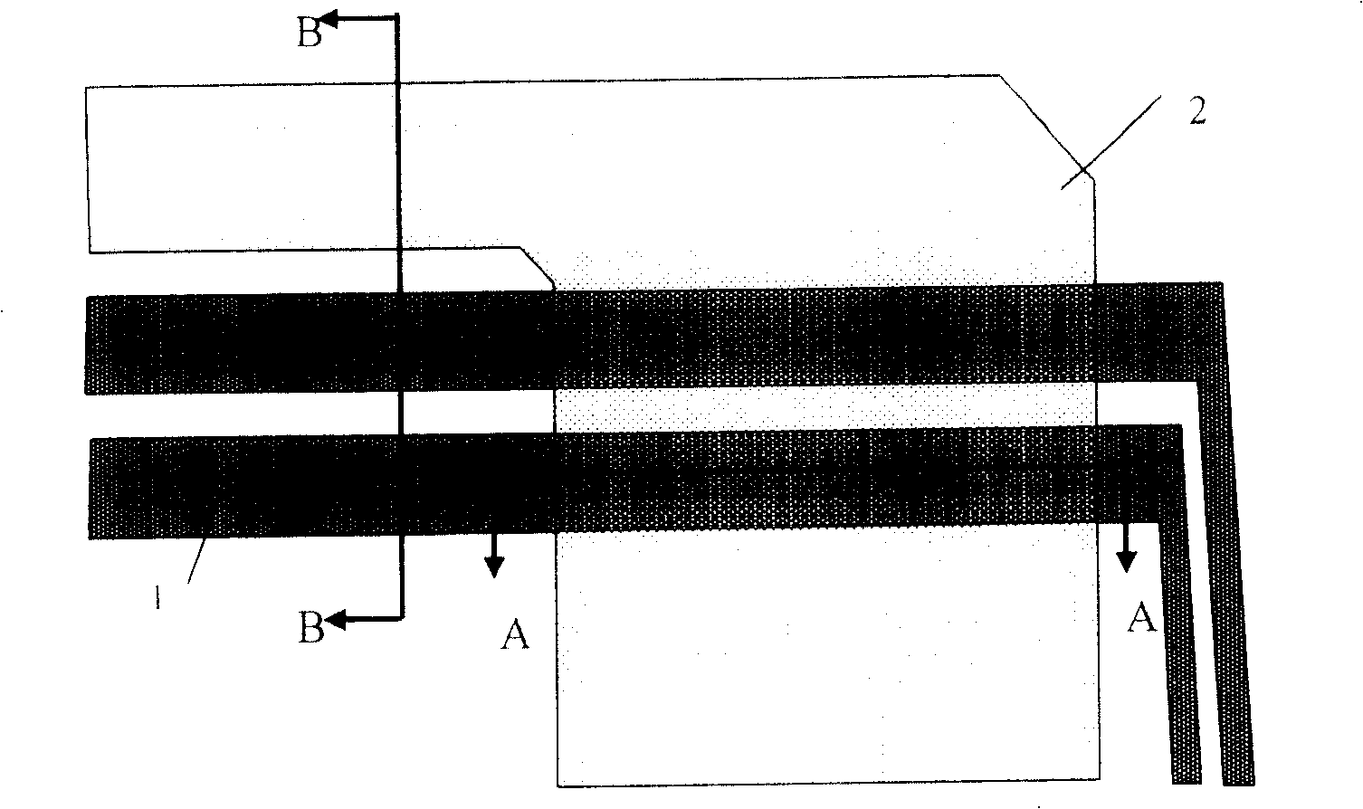
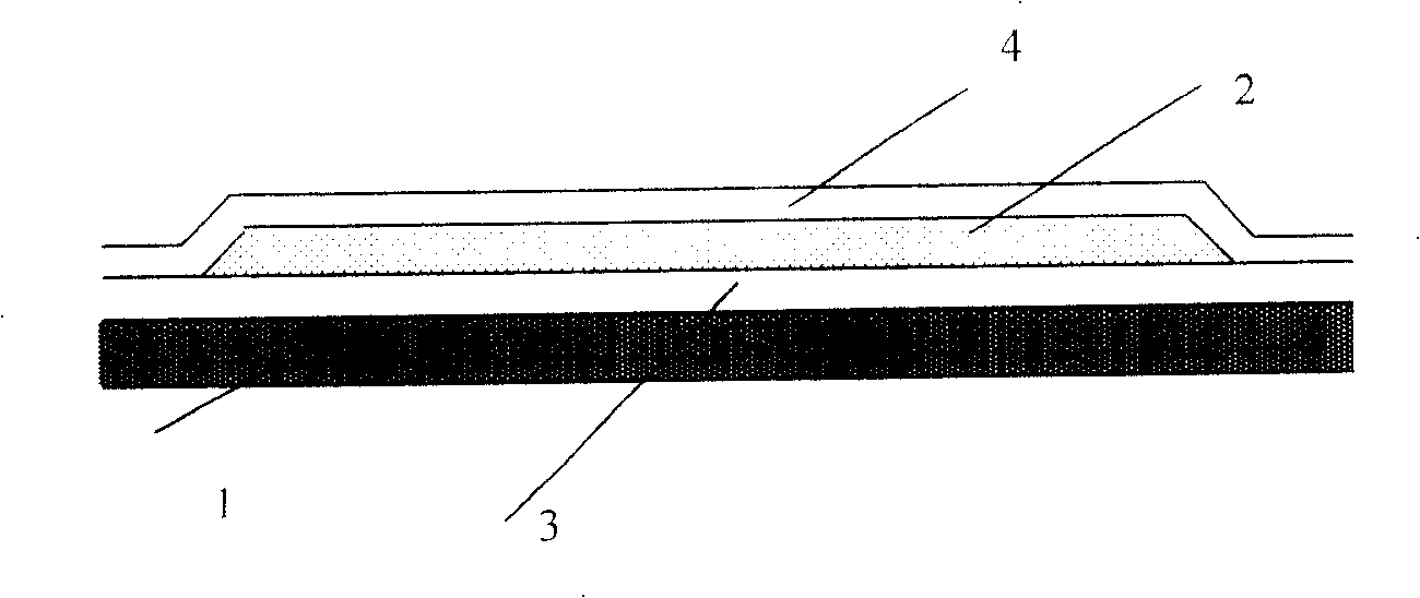
[0048] Figure 4 It is a top view of the structure of the outer common electrode wiring and the repair line in the TFT outer overlapping area of ​​a specific embodiment of the present invention, Figure 4 The cross-sectional view of the C-C position and the D-D position in the middle is as follows Figure 5 and Figure 6 shown. Such as Figure 4 As shown, the structure includes: a TFT substrate (including an array substrate); a set of repair lines 1, generally two, or multiple; a layer of gate insulating layer 3 formed on the repair line 1 The peripheral common electrode wiring 2 is formed on the gate insulating layer 3 and overlaps with the repair line 1 ; the passivation layer 4 is formed on the peripheral common electrode wiring 2 . Wherein, the materials of the repair wire 1 and the peripheral common electrode wire 2 can be one or any combination of molybdenum, aluminum, aluminum-nickel alloy, molybdenum-tungsten alloy, chromium, or copper.

[0049] Such as Figure 4...

Embodiment 2

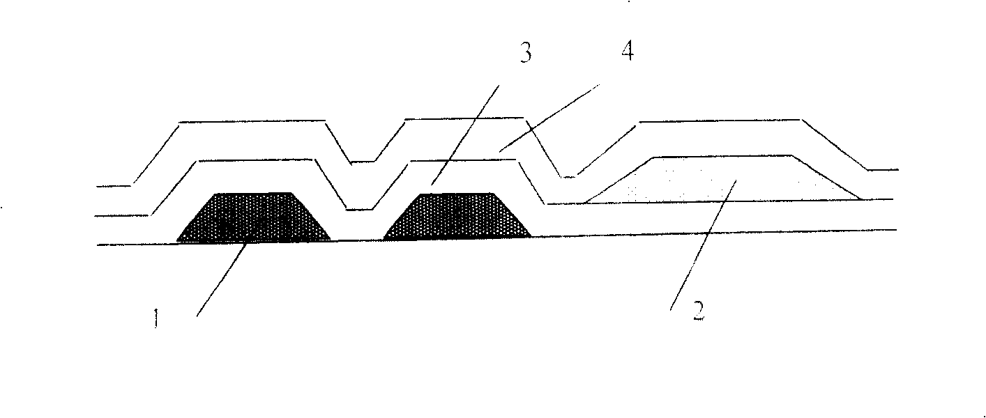
[0058] Figure 7 It is a top view of the outer common electrode wiring and the repair line in the TFT outer overlapping area of ​​another specific embodiment of the present invention, Figure 7 The cross-sectional views of the E-E position and the F-F position in the middle are as follows Figure 8 and Figure 9 shown. Such as Figure 7 As shown, the structure includes: a TFT substrate (including an array substrate); a set of repair lines 1, usually two, or multiple; a gate insulating layer 3, formed on the repair line 1; The electrode wiring 2 is formed on the gate insulating layer 3 and disconnected at the position above the repair line 1; the passivation layer 4 is formed on the peripheral common electrode wiring 2 and is close to the peripheral common electrode wiring 2 A passivation layer via hole or groove 6 is formed at the disconnected position; a connecting lead 5 is formed on the passivation layer 4 and connects the disconnected peripheral common electrode wiring...


PUM


Abstract

This invention discloses a surrounding routing structure of a TFT LCD array base plate including: a base plate and an array structure formed on it, a repairing line formed on the base plate, a grid insulation layer formed on the line, a surrounding public electrode routing formed on the grid insulation layer and overlapped with the repairing wire, in which, the surrounding public electrode routing is in a net structure with the repairing wire crossover region. This invention also discloses another TFT LCD array base plate surrounding routing structure and a manufacturing method for the structure.

Description

technical field [0001] The invention relates to a thin film transistor liquid crystal display (TFT LCD) array substrate structure and a manufacturing method thereof, in particular to a TFT LCD array substrate peripheral wiring structure and a manufacturing method thereof. Background technique [0002] In the structural design of TFT LCD, the layout of TFT (thin film transistor) peripheral wiring, including anti-static conductive ring, gate scanning line, data scanning line, peripheral common electrode wiring, repair line (Repa ir line) and others for The pattern of the test. The existence of these patterns has a great impact on the post-process, such as the box forming process, UV curing of the frame sealant, etc., which may cause defects such as surrounding liquid crystal pollution, poor cutting, ESD, etc. Setting the repair line on the periphery of the TFT is the main method for repairing the disconnection of the data scanning line. After a broken data scanning line is r...

Claims


Application Information

Patent Timeline
Patent Type & Authority Patents(China)
IPC IPC(8): H01L27/12H01L23/522H01L21/84H01L21/768G02F1/136
Inventor 彭志龙
Owner BOE TECH GRP CO LTD
Why Eureka
Try Eureka