
Wiring board and method of producing the same

A technology for wiring substrates and manufacturing methods, applied in semiconductor/solid-state device manufacturing, electrical components, electric solid-state devices, etc., can solve the problems of positioning accuracy obstacles, insufficient connection assistance, and easy occurrence, etc., to improve positioning stability, Good wettability and effective environmental countermeasures

Inactive Publication Date: 2008-10-08
NGK SPARK PLUG CO LTD
View PDF11 Cites 0 Cited by
  • Summary
  • Abstract
  • Description
  • Claims
  • Application Information

AI Technical Summary

Problems solved by technology

Pb-free solder has the following problems: Because of the high reflow temperature, the wettability to Cu series pads is poor. Therefore, even if the solder layer for auxiliary connection is formed by melting, it will not wet and spread well on the surface of the pad, and the solder layer will be exposed. There are many residues on the surface, and the role as a connection aid is not sufficient
In addition, a large amount of Pb-free solder swells high on the pad without wetting and spreading, so it is easy to cause the following problems: when placing and mounting solder balls, the ball will become unstable on the pad, and the positioning Accuracy brings obstacles
In particular, if the amount of solder paste applied is increased to reduce the exposed surface on the pad, this problem is more likely to occur.

Method used


Image

  • Wiring board and method of producing the same
  • Wiring board and method of producing the same
  • Wiring board and method of producing the same

Examples


Embodiment Construction

[0034]Hereinafter, embodiments of the present invention will be described with reference to the drawings.

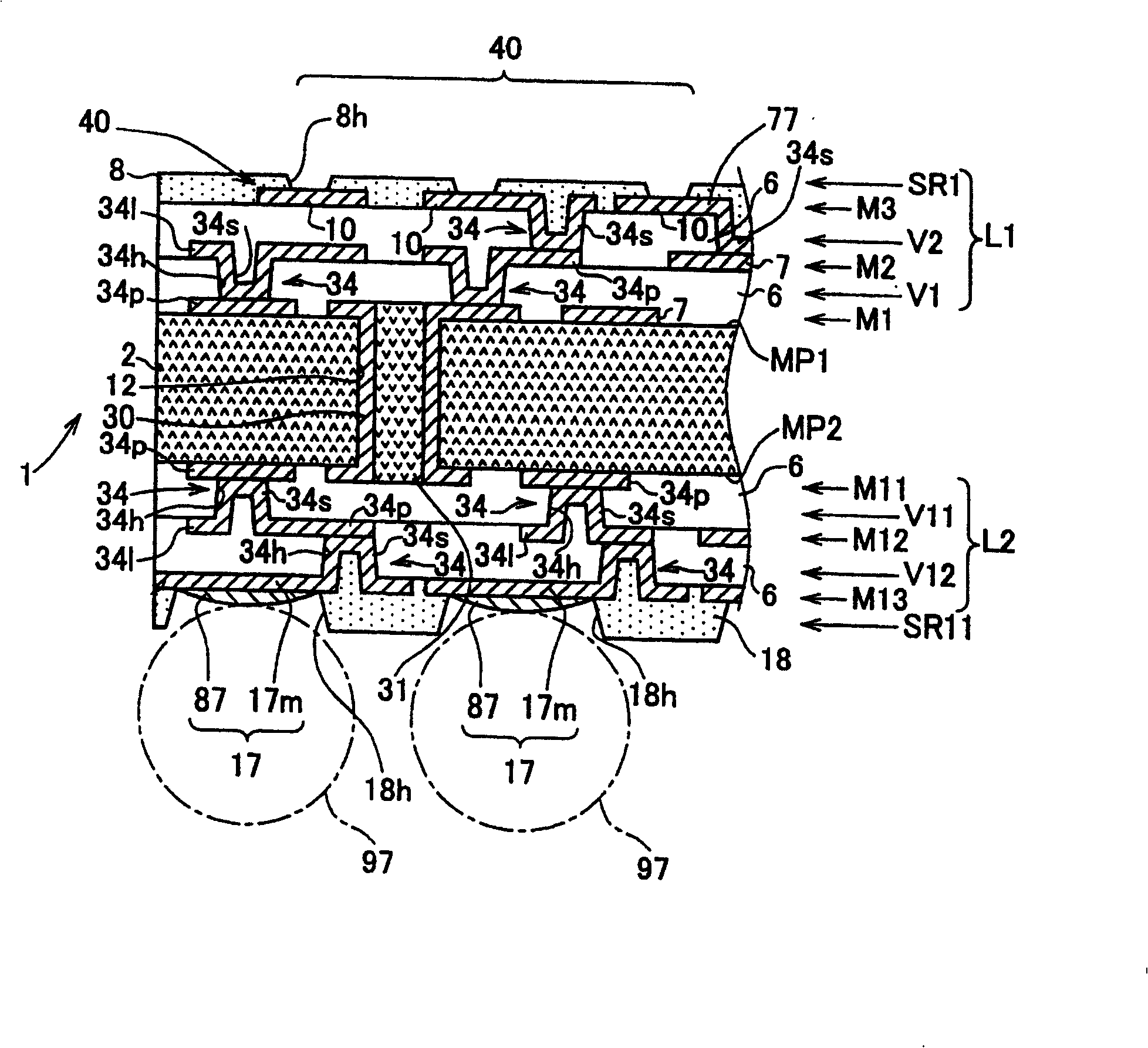
[0035] image 3 It is a figure which schematically shows the cross-sectional structure of the wiring board 1 which concerns on one Embodiment of this invention. The wiring substrate 1 is made of a plate-shaped core 2 made of a heat-resistant resin board (such as a bismaleimide triazine resin board) or a fiber-reinforced resin board (such as a glass fiber-reinforced epoxy resin). Core conductor layers M1 and M11 (referred to as conductor layers) constituting the wiring metal layer are respectively formed on both surfaces of the circuit board according to a predetermined pattern. These core conductor layers M1, M11 are formed as surface conductor patterns covering most of the surface of the plate-shaped core 2, and are used as a power supply layer or a ground layer. On the other hand, a through hole 12 drilled by a punch or the like is formed in the plate-shaped core 2, ...


PUM


Abstract

The invention provides a method for manufacturing a wiring baseplate, which still adopts Sn series high-temperature welding flux with low Pb content and evenly covers Cu series bonding pad surface. The manufacturing method is implemented in the following order: in a pre-plating procedure, a welding flux etching resist layer (18) is formed in an opening part (18h), a main body layer (17m) of a metal bonding pad (17) is exposed, and a Sn series pre-plating layer (91) is utilized to cover the surface of the exposed main body layer (17m); in a coating procedure, welding flux paste (87p) containing welding flux powder which is composed of the Sn series high-temperature welding flux is coated on the Sn series pre-plating layer (91) in the way of being thicker than the Sn series pre-plating layer (91); and in a welding flux fusing procedure, a coating layer of the welding flux paste (87p) on the surface of the Sn series pre-plating layer (91) which covers the main body layer (17m) is heated through a high temperature above the liquidus temperature of the Sn series high-temperature welding flux, the coating layer of the welding flux paste and the Sn series pre-plating layer (91) are fused together and are soaked and spread on the main body layer (17m), therefore forming a Sn series welding flux covering layer (87).

Description

technical field [0001] The present invention relates to a wiring substrate and its manufacturing method. Background technique [0002] Patent Document 1: Japanese Patent Laid-Open No. H10-112514. [0003] Non-Patent Document 1: "Development of High Reliability Sn-Ag Series Lead-Free Solder" Toyota Central Research Institute R&D Review Vol.35 No.2 (2000) p.39. [0004] In an organic package based on a BGA (Ball Grid Array: ball grid array) connection, a solder connection portion constituting the BGA is formed of a solder ball. Generally, solder balls are placed on Cu-based pads formed on a substrate, and a BGA solder connection is formed through reflow processing. Conventionally, high-temperature solder with high Pb content was used as the material of solder balls. High-temperature solder has a high reflow temperature, and its wettability to Cu series pads is also poorer than that of eutectic solder, so it is easy to cause poor connection. Patent Document 1 also discloses...

Claims


Application Information

Patent Timeline
Patent Type & Authority Patents(China)
IPC IPC(8): H01L21/48H01L21/60H01L23/12
Inventor 井场政宏齐木一林贵广
Owner NGK SPARK PLUG CO LTD
Learn More