Electronic beam generator, driving method and image forming device using said device
A technology for image generation and equipment, applied in image communication, image/graphic display tubes, instruments, etc., can solve the problem that the brightness of the displayed graphics deviates from the brightness, etc.
- Summary
- Abstract
- Description
- Claims
- Application Information
AI Technical Summary
Problems solved by technology
Method used
Image

Examples
no. 1 example
[0118] Next, an image display device as a first embodiment of the present invention, and a method of driving the device will be described in detail. First, the structure and operation of the circuit will be described, then the structure and fabrication method of a display panel will be described, and finally the structure and fabrication method of a cold cathode unit included in the display panel will be described.
[0119] (Structure and Operation of Circuits)
[0120] Figure 8 is a circuit diagram showing the configuration of a circuit. shown in Figure 8 There are display panel 201 , scanning circuit 202 , control circuit 203 , shift register 204 , latch circuit 205 , accumulator 206 , memory 207 , multiplier 208 and modulation signal generator 209 .
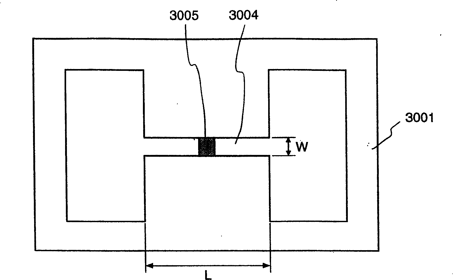
[0121] A group of cold cathode units arranged in rows and columns is included in the display panel 201 . D. x 1~D x m and D y 1~D y n represents feed terminals of m row wirings and n column wirings respectively belon...
no. 2 example
[0228] A second embodiment of the present invention is described below.
[0229] In the first embodiment, each row (D X1 to D Xm ) to be amended. Strictly speaking, however, the voltage distribution in a row close to the column-direction power supply terminals differs from that in a row far from the column-direction power supply terminals due to the influence of column-direction wiring resistance. In order to improve accordingly, it is necessary to carry out corrections which differ from row to row. The second embodiment is proposed from this point of view.
[0230] The structures of the cold cathode unit and the display panel in the second embodiment are similar to those in the first embodiment. The following description focuses on the driving method and correction method of the image display device of the second embodiment. control Figure 27 to describe.
[0231] Figure 27 Reference numeral 201 denotes a display panel, which is similar to that described in the firs...
no. 3 example
[0240] A third embodiment of the present invention will be described below with reference to the accompanying drawings.
[0241] First, the operation method for determining the correction value is described, and then the structure and operation of the third embodiment are described.
[0242] (method of calculating correction value)
[0243] A calculation method of a correction value (correction voltage) for correcting a loss (voltage drop) caused by wiring resistance will now be described. It should be noted that the following calculation method is applied when measuring the correction rate in the first and second embodiments.
[0244] For example, adding Figure 32 The voltage on each unit shown in , drops with the amount of current flowing into the wiring. It should be pointed out that Figure 32 The case where all the cold cathode units (D1-Dn) of the unit in the mth row are driven is listed, that is, the case where all the pixels in the mth row in the image are turned ...
PUM
 Abstract
Description
Claims
Application Information