

Method for manufacturing semiconductor device
A semiconductor and device technology, applied in the field of semiconductor equipment, can solve the problem of serious damage to TFT, and achieve the effect of reliable semiconductor equipment and preventing damage
- Summary
- Abstract
- Description
- Claims
- Application Information
AI Technical Summary
Problems solved by technology
Method used
Image

Examples
Embodiment approach
[0073] Embodiments of the present invention will be described below with reference to the accompanying drawings. However, it is easily understood by those skilled in the art that the present invention can be employed in many ways and obviously has various changes and modifications unless such changes and modifications depart from the purpose and scope of the present invention. Therefore, interpretation of the present invention is not limited to the description of the present embodiment.
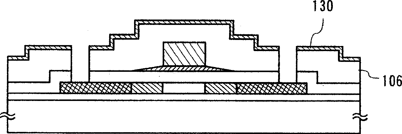
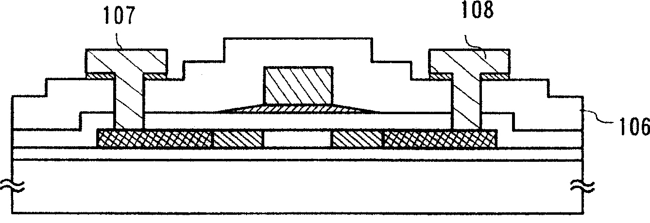
[0074] Refer to the attached Figures 1A to 1D , Figures 2A to 2C and image 3 A manufacturing process of the semiconductor device according to the present embodiment is described.
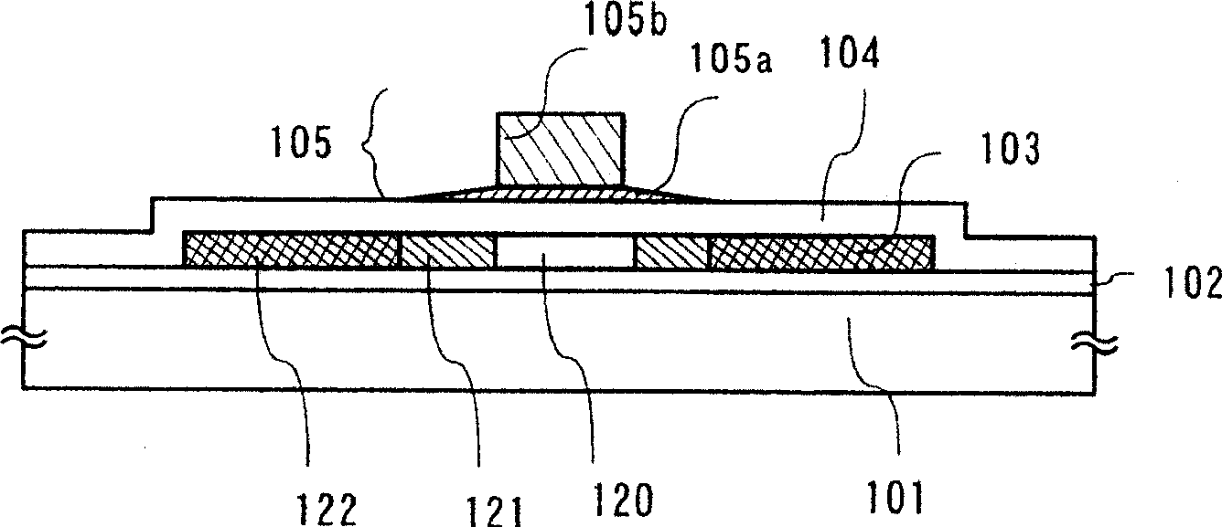
[0075] First, thin film transistors (TFTs) are fabricated. A base film 102, a semiconductor layer 103 as an active layer, a gate insulating film 104, and a gate electrode 105 are formed on a substrate 101 ( Figure 1A ).
[0076] A substrate having an insulating film formed on its surface such as a glass su...
Embodiment 1
[0110] In this embodiment, a TFT in which a contact hole is formed with a metal cap film and a TFT in which a contact hole is not formed with a metal cap film are compared in terms of transistor characteristics, see FIGS. 4A and 4B, Figures 5 to 8 , and Figures 29A and 29B.
[0111] Fig. 29A shows gate voltage and drain current characteristics of an n-channel TFT fabricated without forming a metal cap film. FIG. 4A shows gate voltage and drain current characteristics of an n-channel TFT fabricated when a metal cap film is formed.
[0112] In FIGS. 4A and 29A , the horizontal axis represents the gate voltage (VG[V]), and the vertical axis represents the drain current (ID[A]).
[0113] In FIGS. 4A and 29A, the channel length (L) and channel width (W) of the n-channel TFT are 3 μm and 2 μm, respectively, and the thickness of the gate insulating film (referred to as “Tox” in this specification) is 55 nm.
[0114] In FIG. 4A and FIG. 29A, the TFT characteristics before the conta...
Embodiment 2
[0145] This embodiment describes a method for manufacturing an active-matrix liquid crystal display in which reverse-staggered TFTs are used as switching elements. In addition, cross-sectional views of the manufacturing process are shown in FIGS. 9A to 9E, respectively, and Figure 10 Represents a top view.
[0146] First, a bottom insulating film 611 is formed on a substrate 610 . It is preferable to use an insulating film such as a silicon oxide film, a silicon nitride film, or a nitrogen-containing silicon oxide film (SiO x N y ) as the bottom insulating film 611. In addition to the non-alkaline glass substrate, a heat-resistant plastic substrate capable of withstanding the processing temperature in the manufacturing process can also be used as the substrate 610 . In a reflective liquid crystal display, a semiconductor substrate such as single crystal silicon, a metal substrate such as stainless steel, or a ceramic substrate with an insulating layer on its surface may a...
PUM
| Property | Measurement | Unit |
|---|---|---|
| thickness | aaaaa | aaaaa |
| thickness | aaaaa | aaaaa |
| thickness | aaaaa | aaaaa |
Abstract
Description
Claims
Application Information