A low voltage and high gain charge circuit

A charge pump, high gain technology, applied in logic circuits, electrical components, conversion equipment without intermediate conversion to AC, etc., to ensure the voltage gain, promote forward current, and achieve the effect of effective control

Inactive Publication Date: 2009-04-15
NANJING UNIV
View PDF6 Cites 0 Cited by
  • Summary
  • Abstract
  • Description
  • Claims
  • Application Information

AI Technical Summary

Problems solved by technology

When the type and size of the power tube are determined, to further improve the on-resistance, the only solution is to increase V GS

Method used


Image

  • A low voltage and high gain charge circuit
  • A low voltage and high gain charge circuit
  • A low voltage and high gain charge circuit

Examples


Embodiment Construction

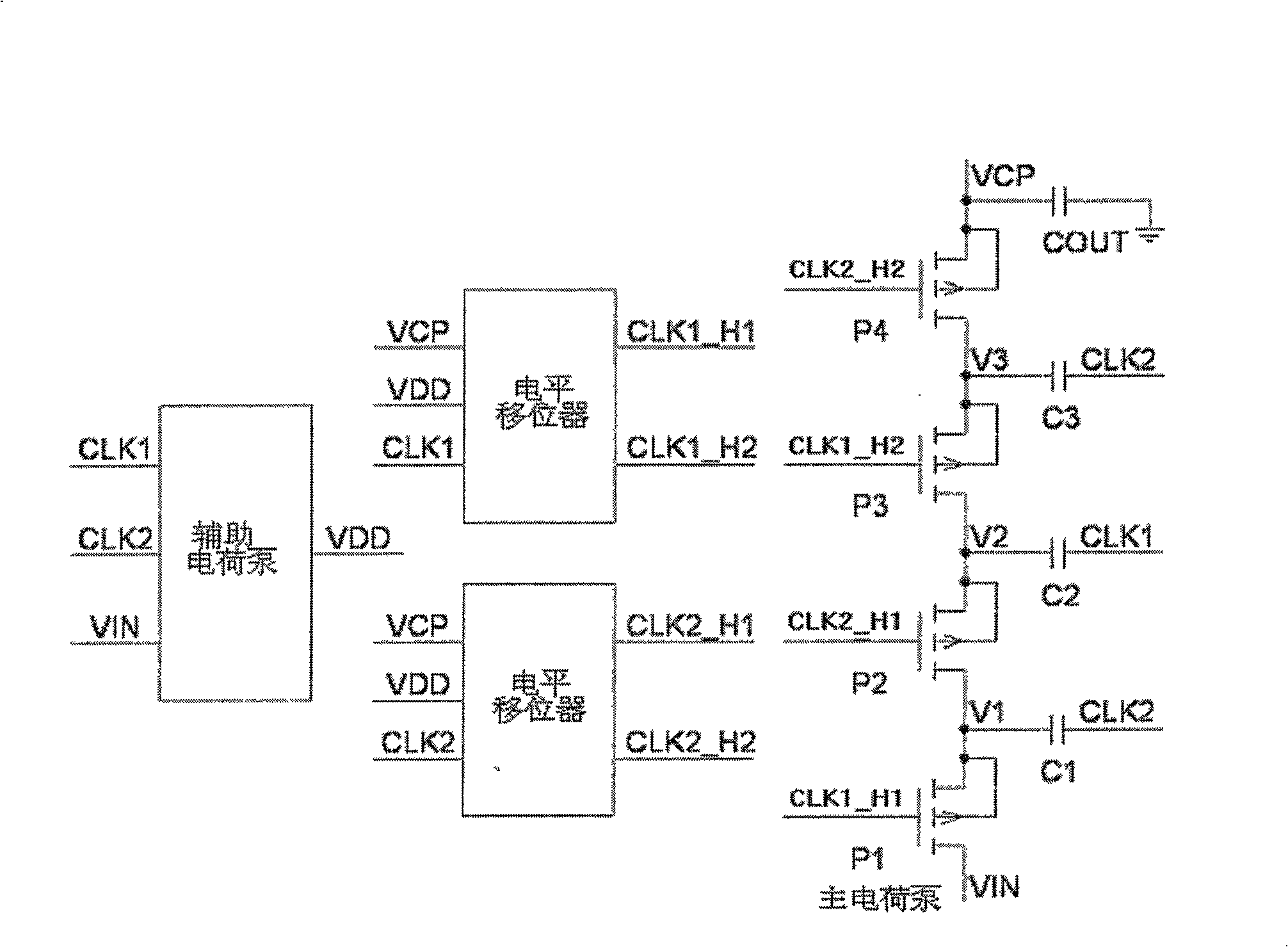
[0041] In order to have a further understanding of the structure and principle of the circuit of the present invention, a detailed introduction will be made below in conjunction with the accompanying drawings.

[0042] image 3 It is an example of the charge pump circuit of the present invention. It includes three parts, auxiliary charge pump, level shifter and main charge pump. The auxiliary charge pump provides the second high level (VDD) for the level shifter, and is used to improve the swing of the main charge pump low-order switch (P1, P2) control clock and accelerate its startup process; Provides the highest level (VCP) to the level shifter, which ultimately improves the swing of the control clock for the main charge pump high-order switches (P3, P4).

[0043] The auxiliary charge pump generates a double-increased level (VDD=2VIN), the main electric pump generates a four-fold multiplied level (VCP=4VIN), and the two level shift circuits in the middle realize the transi...


PUM


Abstract

The invention discloses a circuit structure of charge pump comprising an auxiliary charge pump, a level shifter, and a main charge pump. The auxiliary charge pump provides the level shifter with a sub-high level (VDD) and can be used to improve the swing of the controlling clock of the main charge pump low level switches (P1, P2) to speed up starting of the main charge pump. The main charge pump provides the level shifter with the highest level (VCP) after starting so that the swing of the controlling clock of the main charge pump high level switches (P3, P4) can be improved eventually. The invention can effectively control the conductance of the switch tube; improve the voltage gain; overcome the defects of low efficiency and long time for starting the high level charge pump, and is characterized in high voltage gain and short time for starting, applicable for low-voltage applied environment.

Description

technical field [0001] The invention relates to a conversion circuit from low voltage to high voltage, in particular to a low voltage, high gain charge pump circuit. Background technique [0002] The charge pump occupies an important position in the field of analog circuits. It can realize the transition from low voltage to high voltage, so it can reduce the requirement of system supply voltage input swing without affecting the demand of higher voltage application in the system. This is especially important in the era of deep submicron integrated circuit design. [0003] Low Dropout voltage regulator (LDO) is the most commonly used type of DC-DC power modulator in power management chips. When designing a low dropout voltage regulator (LDO) chip, it is necessary to solve the problem of LDO ultra-low pressure drop problem. [0004] figure 1 A commonly used LDO system structure is given, which is composed of error amplifier, reference circuit, power transistor, feedback circ...

Claims


Application Information

Patent Timeline
Patent Type & Authority Patents(China)
IPC IPC(8): H02M3/07H03K19/094
Inventor 高明伦杨盛光何书专李丽李伟潘红兵
Owner NANJING UNIV
Why Eureka
Try Eureka