Making technology method for flash memory

A manufacturing process and flash memory technology, which is applied in the field of semiconductor integrated circuit technology, achieves the effects of small impact, improved rewritable performance, and beneficial to subsequent processes

Active Publication Date: 2009-05-20
SHANGHAI HUAHONG GRACE SEMICON MFG CORP +1
View PDF4 Cites 0 Cited by
  • Summary
  • Abstract
  • Description
  • Claims
  • Application Information

AI Technical Summary

Problems solved by technology

[0002] As a main non-volatile memory, flash memory has a wide range of uses in smart cards, microcontrollers and other fields. Compared with EEPORM, another non-volatile memory, flash memory has obvious advantages in area, but at the same time, flash memory The reliability, especially the number of rewritable times, is worse than that of EEPROM, so it has not been used in bank cards, ID cards and other products

Method used


Image

  • Making technology method for flash memory
  • Making technology method for flash memory
  • Making technology method for flash memory

Examples


Embodiment Construction

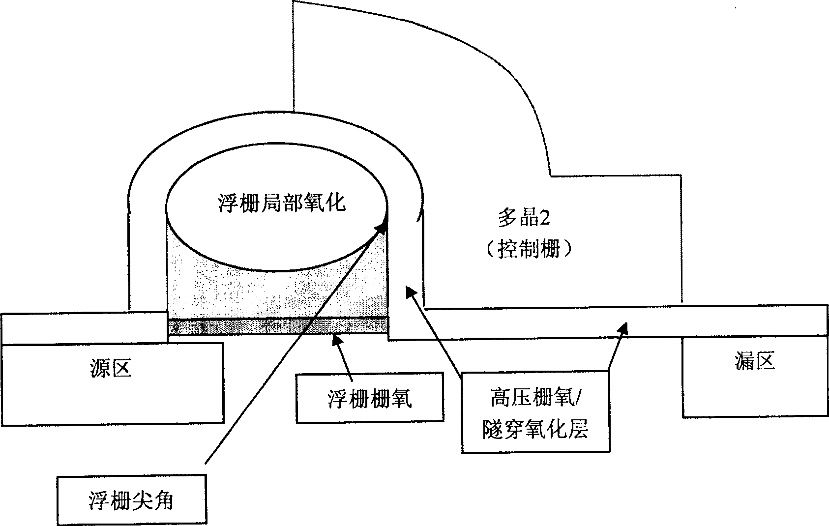
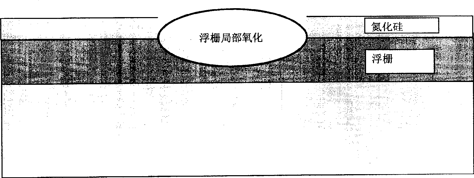
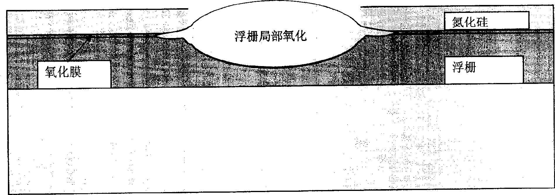
[0015] The main process steps that the present invention adopts are as follows: 1. isolation region / active area forms (same as existing technology); 2. high-voltage transistor, memory cell well implantation (same as existing technology); 3. floating gate oxidation (same as existing technology); with craftsmanship, ); 4. floating gate polycrystalline deposition (with existing technology, ); 5. A thin layer of oxide film is grown on the surface of the floating gate for about 6. Silicon nitride deposition; 7. Partial oxidation of the floating gate (same as the existing process); 8. Etching of the floating gate (same as the existing process); 9. The subsequent steps are also the same as the existing process.

[0016] The present invention compares with existing technology: steps 1~4 are the same as existing technology, after floating gate is oxidized, deposit a layer of polysilicon on the surface; Then add a process procedure, promptly grow a layer on the surface of polysilico...


PUM


Abstract

The invention discloses a method of manufacturing a flash memory. In the prior flash memory process, after floating boom polycrystal deposits, the floating boom generates a thin oxide film with the thickness of 20-50 . The invention can effectively control the beak shape with partial oxidization, expand process window and is good for floating boom sharp corner control, stability, evenness and the whole chip erasing performance improvement.

Description

technical field [0001] The invention relates to a semiconductor integrated circuit process method, in particular to a flash memory manufacturing process method. Background technique [0002] As a main non-volatile memory, flash memory has a wide range of uses in smart cards, microcontrollers and other fields. Compared with EEPORM, another non-volatile memory, flash memory has obvious advantages in area, but at the same time, flash memory The reliability, especially the erasable number of times, is worse than that of EEPROM, so it has not been used in products such as bank cards and ID cards. [0003] SST flash memory is a type of flash memory invented by Bing Yeh in 1990 (US Patent No. 5029130), and the structure of its storage unit is as follows figure 1 As shown, among them, the polycrystalline one is a floating gate, and the following is 80-90 Thick floating gate oxide; a part of polycrystalline 2 covers the floating gate as the control gate during erasing, and the thi...

Claims


Application Information

Patent Timeline
Patent Type & Authority Patents(China)
IPC IPC(8): H01L21/8247H01L21/336H01L21/28H01L27/11521
Inventor 杨斌龚新军李铭
Owner SHANGHAI HUAHONG GRACE SEMICON MFG CORP
Why Eureka
Try Eureka