

Testing structure for MOS capacitor and location method for failure point
A technology of capacitance testing and positioning method, which is applied in the direction of electronic circuit testing, non-contact circuit testing, semiconductor/solid-state device testing/measurement, etc. It can solve problems such as labor-intensive, time-consuming, and cost-increasing problems, and avoid repeated cutting and production The process is simple and the effect of increasing production cost
- Summary
- Abstract
- Description
- Claims
- Application Information
AI Technical Summary
Problems solved by technology
Method used
Image

Examples
no. 1 example
[0044] As the first embodiment illustrating the method of the present invention, the specific implementation steps of applying the method of the present invention to locate the failure point and perform failure analysis are:
[0045] First, a test MOS capacitor is formed.
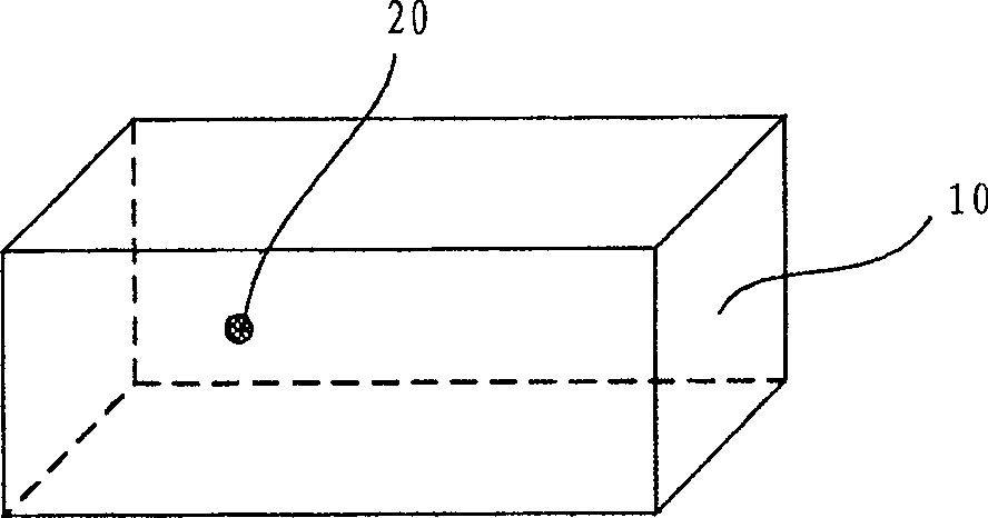
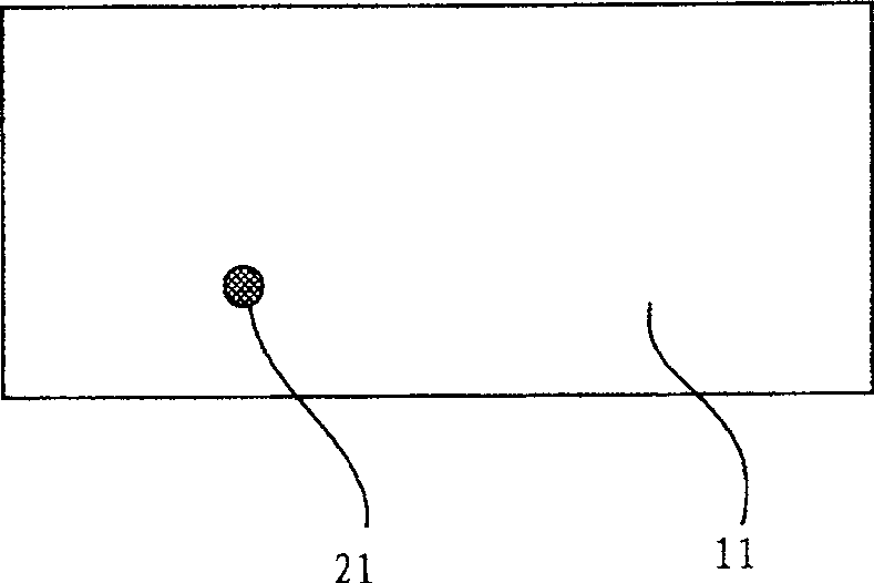
[0046] The test MOS capacitor is formed simultaneously with the normal product and has the same structure; the test MOS capacitor is formed on the dicing line in the wafer; for the convenience of failure point detection, the test MOS capacitor grid size can be designed to be large enough, as the method of the present invention In an embodiment, the gate size of the test MOS capacitor is selected as: 50 microns*50 microns.
[0047] Admittedly, the determination of the gate size of the test MOS capacitor is a special choice made for the convenience of describing the specific embodiments of the present invention, and should not be used as a limitation to the implementation of the method of the present inventio...
no. 2 example
[0064] As the second embodiment of the present invention, the specific implementation steps of applying the method of the present invention to locate the failure point and perform failure analysis are as follows:
[0065] First, a test MOS capacitor is formed.
[0066] The test MOS capacitor is formed simultaneously with the normal product and has the same structure; the test MOS capacitor is formed on the dicing line in the wafer; for the convenience of failure point detection, the test MOS capacitor grid size can be designed to be large enough, as the method of the present invention In an embodiment, the gate size of the test MOS capacitor is selected as: 50 microns*50 microns.
PUM
 Abstract
Description
Claims
Application Information