Supercharge Your Innovation With Domain-Expert AI Agents!

Semiconductor structure

A semiconductor and conductive type technology, applied in semiconductor devices, electrical solid devices, electrical components, etc., can solve problems such as component reliability and output resistance, and achieve the effect of improving reliability and reducing P-type impurity atoms

Active Publication Date: 2009-06-10
TAIWAN SEMICON MFG CO LTD
View PDF3 Cites 0 Cited by
  • Summary
  • Abstract
  • Description
  • Claims
  • Application Information

AI Technical Summary

Problems solved by technology

It indicates output resistance issues that will cause component reliability issues

Method used


Image

  • Semiconductor structure
  • Semiconductor structure
  • Semiconductor structure

Examples


Embodiment

[0054] Figure 3 to Figure 8A A preferred embodiment of the invention is shown, and variations of the preferred embodiment will be discussed next.

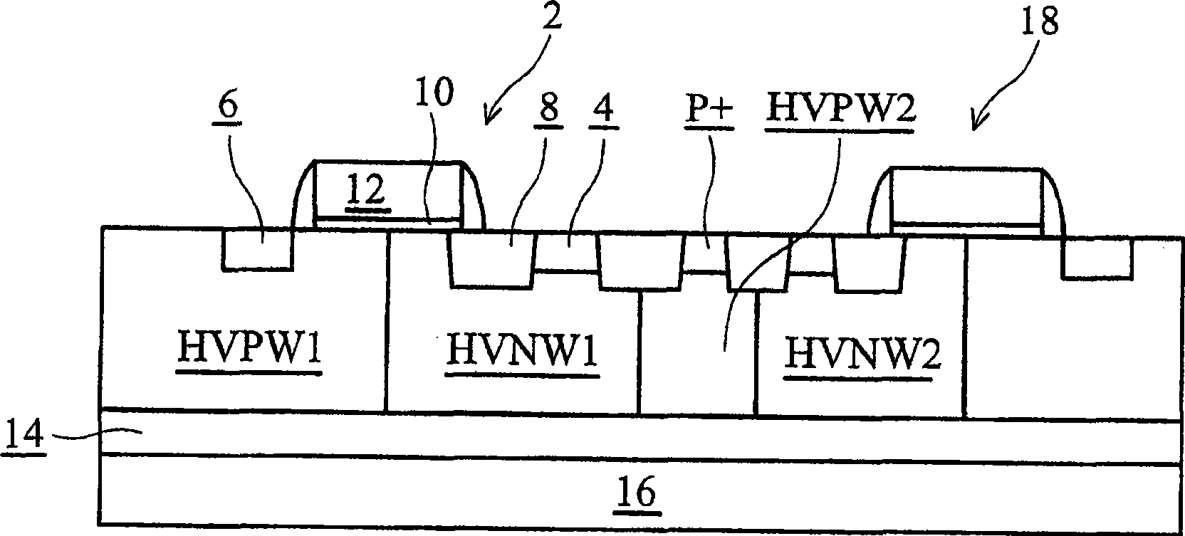
[0055] refer to image 3 , image 3 A substrate 20 is provided. Substrate 20 preferably includes a semiconductor material such as silicon, however other semiconductor materials may be used for substrate 20 . Preferably, the substrate 20 is lightly doped with P-type impurities, but the substrate 20 can also be lightly doped with N-type impurities.

[0056] Photoresist 22 is formed and patterned using etching techniques. The high-voltage anti-punch-through region 24 is formed, which is also called the high-voltage N-type anti-punch-through region HVNAPT, because the reverse region in the high-voltage anti-punch-through region 24 is N-type. The high-voltage N-type anti-punching region 24 is preferably doped with P-type impurities, such as boron and / or indium. Preferably, the concentration of the P-type impurity in the high-volt...


PUM


Abstract

A semiconductor structure includes a first high-voltage well (HVW) region of a first conductivity type overlying a substrate, a second HVW region of a second conductivity type opposite the first conductivity type overlying the substrate and laterally adjoining the first HVW region, and a third HVW region of the second conductivity type underlying the second HVW region. A region underlying the first HVW region is substantially free from the third HVW region, wherein the third HVW region has a bottom lower than a bottom of the first HVW region. The semiconductor structure further includes an insulation region in a portion and extending from a top surface of the first HVW region into the first HVW region, a gate dielectric extending from over the first HVW region to over the second HVW region wherein the gate dielectric has a portion over the insulation region, and a gate electrode on the gate dielectric.

Description

technical field [0001] The present invention relates to a semiconductor device, in particular to a metal oxide semiconductor (MOS) device, and more particularly to a structure and a manufacturing method of a high voltage metal oxide semiconductor device. Background technique [0002] High-voltage metal-oxide-semiconductor devices are widely used in many electronic devices, such as input / output circuits, central process unit (CPU) power supplies, power management systems, and AC / DC converters. [0003] There are many different types of high voltage metal oxide semiconductor components. The symmetrical high voltage metal oxide semiconductor device has a symmetrical structure at the source terminal and the drain terminal, and high voltage can be applied at the source terminal and the drain terminal. The asymmetric HVMOS device has an asymmetric structure at the source terminal and the drain terminal. For example, only one of the source terminal and the drain terminal, traditi...

Claims


Application Information

Patent Timeline
Patent Type & Authority Patents(China)
IPC IPC(8): H01L29/78H01L27/04
Inventor 黄坤铭周学良朱翁驹吴成堡
Owner TAIWAN SEMICON MFG CO LTD
Features
  • R&D
  • Intellectual Property
  • Life Sciences
  • Materials
  • Tech Scout
  • Unparalleled Data Quality
  • Higher Quality Content
  • 60% Fewer Hallucinations
Learn More