
Sampling/retaining circuit device

A technology for holding circuits and holding capacitors, which is applied in circuits, electrical components, electronic switches, etc., can solve problems such as voltage value errors, achieve convenient implementation, simple circuit structure, and improve the effect of incorrect output levels

Inactive Publication Date: 2009-06-24
INST OF SEMICONDUCTORS - CHINESE ACAD OF SCI
View PDF6 Cites 0 Cited by
  • Summary
  • Abstract
  • Description
  • Claims
  • Application Information

AI Technical Summary

Problems solved by technology

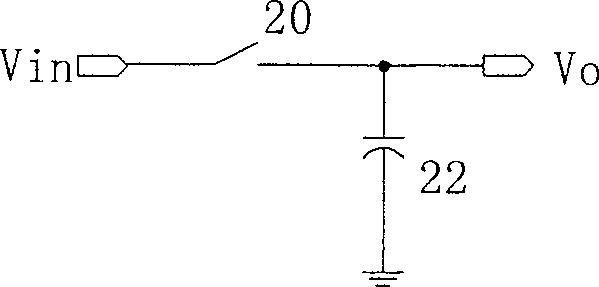
When the switch 20 is turned off, some of these charges are deposited on the capacitor 22, which causes errors in the voltage value stored on the capacitor 22.

Method used


Image

  • Sampling/retaining circuit device
  • Sampling/retaining circuit device
  • Sampling/retaining circuit device

Examples


Embodiment Construction

[0015] The embodiments of the present invention will be described in detail below in conjunction with the accompanying drawings.

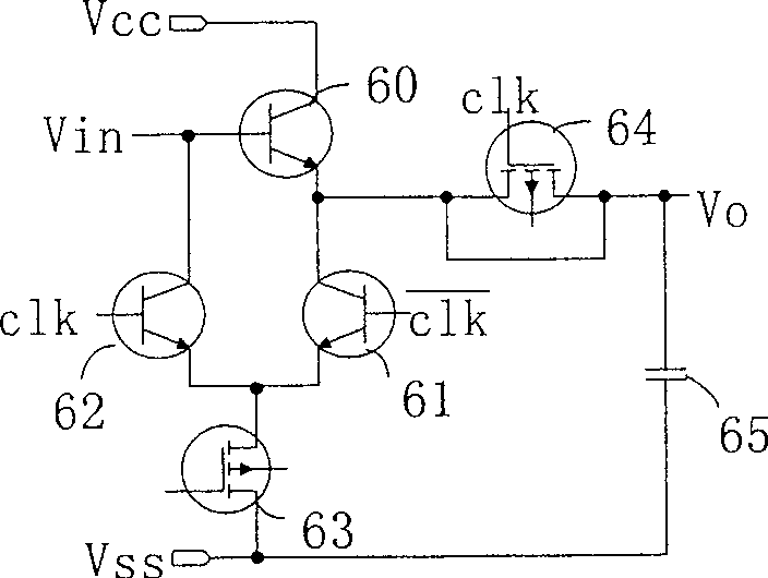
[0016] The principle device of the switched capacitor sample / hold circuit proposed by the present invention is as image 3 As shown, the NPN type bipolar junction transistor 60, the NPN type bipolar junction transistor 61, the NPN type bipolar junction transistor 62 and the N-channel field effect transistor 63 form a sample / hold switch, and the N-channel field effect transistor 64 For the compensation circuit, the capacitor 65 is a holding capacitor. The working principle of the circuit is as follows: The gate of the N-channel field effect transistor 64 is connected to the bias level, so that it can provide the NPN type bipolar junction transistor 62 and the NPN type bipolar junction transistor 61 when one of them is turned on. The required current. When the clock signal clk is low, the NPN bipolar junction transistor 62 is turned off, and the NPN bipo...


PUM


Abstract

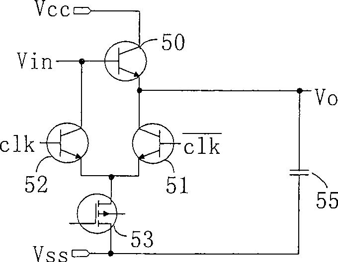
The invention relates to a sample / hold circuit device which comprises a hold capacitor and a sample / hold switch device, wherein, the sample / hold switch device is a biasing circuit device which is formed by three NPN type bipolar junction transistors and a N slot field-effect transistor, one end of the sample / hold switch device is connected to an analog or radio-frequency signal source, the other end of the sample / hold switch device is connected to the hold capacitor; base electrodes of two NPN bipolar junction transistors are respectively connected to two complementary sample / hold clock signals, the emitters of the two NPN bipolar junction transistors are connected with each other and connected to the drain electrode of the N slot field-effect transistor, and the collector electrodes of the two NPN bipolar junction transistors are respectively connected with the base electrode and the emitter of the third NPN type bipolar junction transistor; the collector electrode of the third NPN type bipolar junction transistor is connected with a power supply; the source electrode of the N slot field-effect transistor is connected with the earth and the grid electrode is connected with bias voltage; a compensating circuit device is connected between the sample / hold switch device, which can effectively solve the problem of incorrectness of output level caused by charge injection.

Description

Technical field [0001] The present invention relates to a sample / hold circuit device, in particular to a sample / hold circuit device used in an analog / digital converter. Background technique [0002] A simple switched capacitor sample / hold circuit can be used to convert between the analog continuous time domain and the sampled data domain. Its function is to track and sample the analog input signal and keep the sampled value at a certain level according to the needs of subsequent signal processing. time. figure 1 The schematic diagram of the schematic diagram shows a simple switched capacitor sample / hold circuit in which an input analog signal Vin is applied to a switch 20 that is opened and closed at a periodic clock frequency. The capacitor 22 is connected between the output terminal of the switch 20 and the common ground, and generates an output voltage at both ends thereof. The capacitor 22 is generally a linear polymer-polymer (poly-poly) or metal-metal capacitor. The output...

Claims


Application Information

Patent Timeline
Patent Type & Authority Patents(China)
IPC IPC(8): G11C27/02H03K17/51H03K17/60H03K17/687H03M1/12
Inventor 朱旭斌石寅
Owner INST OF SEMICONDUCTORS - CHINESE ACAD OF SCI
Learn More