Making method for storage capacitor

A technology for storage capacitors and manufacturing methods, which is applied in semiconductor/solid-state device manufacturing, circuits, electrical components, etc., can solve problems such as capacitor manufacturing failure and storage capacitor capacity reduction, so as to reduce electrical failures, reduce defects, The effect of high robustness

Active Publication Date: 2009-07-22
SEMICON MFG INT (SHANGHAI) CORP +1
View PDF5 Cites 0 Cited by
  • Summary
  • Abstract
  • Description
  • Claims
  • Application Information

AI Technical Summary

Problems solved by technology

During the baking process of the subsequent process, the air in the air gap 119a expands due to heat and explodes, causing the failure of the capacitor to be manufactured.
Reducing the depth of the groove 106a can avoid the formation of the air gap 119a, but the surface area of ​​the capacitor plate is sacrificed to reduce the capacity of the storage capacitor

Method used


Image

  • Making method for storage capacitor
  • Making method for storage capacitor
  • Making method for storage capacitor

Examples


Embodiment Construction

[0048] The specific embodiments of the present invention will be described in detail below in conjunction with the accompanying drawings.

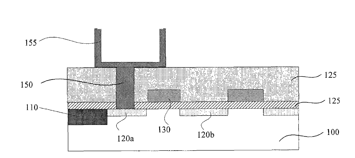
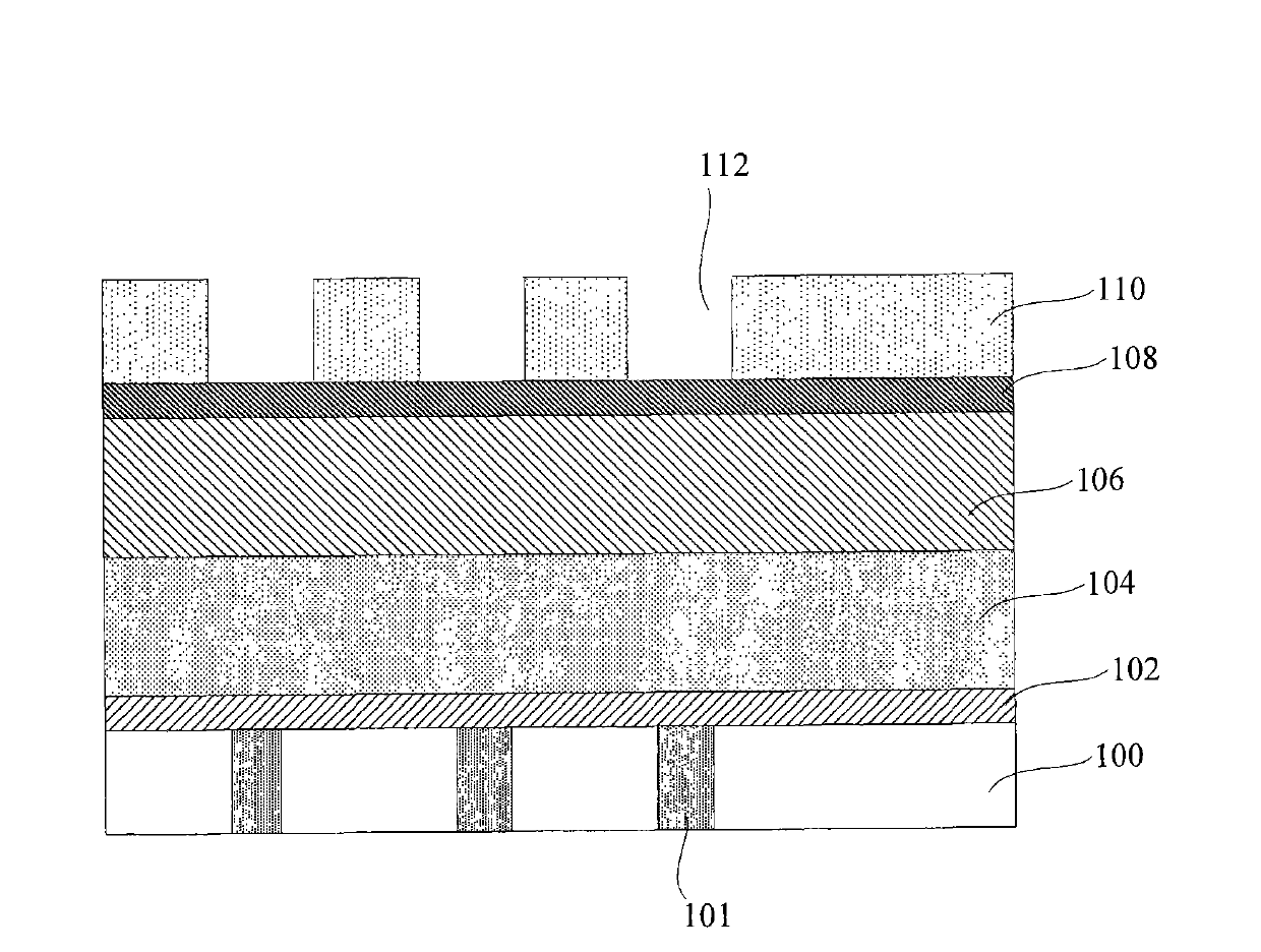
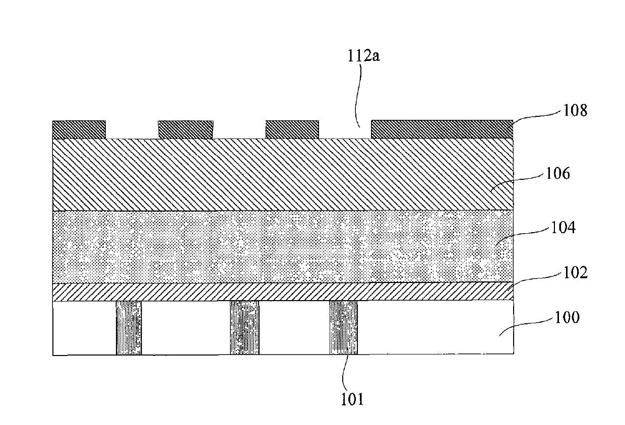
[0049] Figure 11 It is a flowchart of a manufacturing method according to an embodiment of the present invention. Such as Figure 11 Shown, first. A semiconductor substrate is provided on which a device layer, such as a metal oxide semiconductor transistor, is formed. An insulating layer such as silicon oxide is deposited on the device, a connection hole is formed in the insulating layer, the connection hole is filled with a conductive substance, and the bottom of the connection hole is connected to the source of the transistor (S300).

[0050] A first dielectric layer is formed on the insulating layer (S310); the material of the first dielectric layer may be borophosphosilicate glass (BPSG).

[0051] A first conductive layer is formed on the first dielectric layer (S320), and the first conductive layer may be polysilicon.

[0052] A...


PUM


Abstract

A method for manufacturing a storage capacitor, comprising: forming a first dielectric layer on an insulating layer of a substrate; forming a first conductive layer on the first dielectric layer; selectively etching the first conductive layer and The first dielectric layer forms a groove, and the bottom of the groove exposes the surface of the insulating layer; a second dielectric layer is formed on the side wall of the groove; a second conductive layer is formed on the bottom of the groove and the surface of the second dielectric layer ; forming a third dielectric layer on the sidewall and above the second conductive layer in the trench; filling the third conductive layer on the first conductive layer and the third dielectric layer in the trench. The manufacturing method avoids the defect that capacitor plates collapse during the manufacturing process.

Description

technical field [0001] The invention relates to the technical field of semiconductor manufacturing, in particular to a method for manufacturing a storage capacitor. Background technique [0002] A DRAM storage unit generally includes a storage capacitor and a MOS transistor. The increase of its storage density needs to integrate more storage units per unit area and store more information per unit storage unit. The integration of more memory cells per unit area depends on the reduction of device size and the progress of lithography technology; for storing more information per unit memory cell, in addition to looking for high dielectric constant materials and reducing the distance between capacitor plates, most people currently use The method of increasing the surface area of ​​the plate, for example, the capacitor plate is designed in the shape of a barrel, a column, a crown, etc. to increase the area of ​​the plate. Chinese patent application No. 98118488.X proposes a meth...

Claims


Application Information

Patent Timeline
Patent Type & Authority Patents(China)
IPC IPC(8): H01L21/00H01L21/02H01L21/82H01L21/8222H01L21/8242
Inventor 黄子伦
Owner SEMICON MFG INT (SHANGHAI) CORP
Why Eureka
Try Eureka