

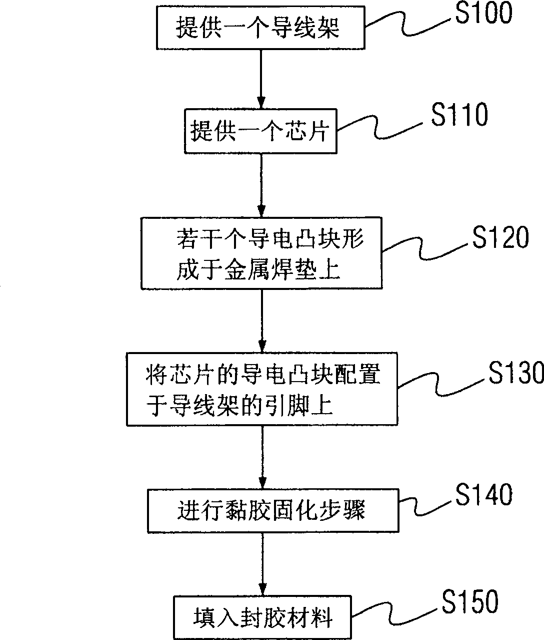
Semiconductor packaging structure with intensification layer and encapsulation method thereof
A packaging structure and packaging method technology, which is applied in semiconductor devices, semiconductor/solid-state device manufacturing, semiconductor/solid-state device components, etc., can solve problems such as loss of chip packaging purpose, bump cracking, eutectic tin-lead bump collapse, etc. , to achieve the effect of increasing electrical conductivity, avoiding collapse, and strengthening mechanical strength
- Summary
- Abstract
- Description
- Claims
- Application Information
AI Technical Summary
Problems solved by technology
Method used
Image

Examples
Embodiment Construction
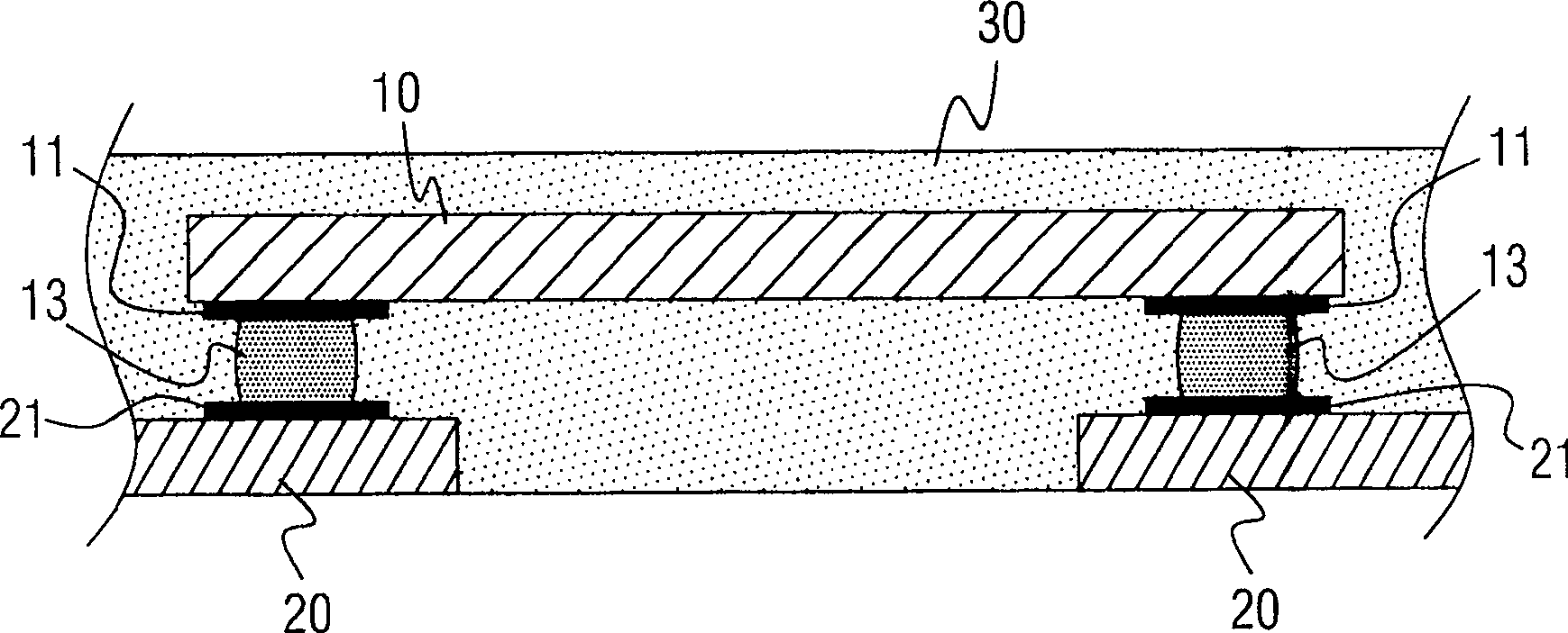
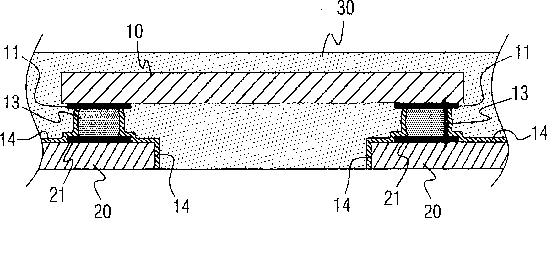
[0026] Please refer to Figure 3A , Figure 3A It is a schematic diagram of a semiconductor package structure with a strengthening layer according to the present invention. The semiconductor package structure includes a lead frame 20 with several pins 21, a chip 10 and several conductive bumps 13, wherein the surface of the chip 10 has several metal solder joints. The pads 11 and the conductive bumps 13 are used to connect the metal pads 11 of the chip 10 and the pins 21 of the lead frame 20 . The components of the conductive bumps 13 include gold, copper, lead, tin or silver. These conductive bumps 13 also respectively include several conductive adhesives, and the components of the conductive adhesives include lead, tin, copper or silver.
[0027] A strengthening layer 14 is covered on the surface of the pin 21 and the conductive bump 13, or this strengthening layer 14 can only cover the surface of the conductive adhesive of the conductive bump 13, it can be a metal layer, a...
PUM
 Abstract
Description
Claims
Application Information