Salicide process using cmp for image sensor

An image sensor and metal silicide technology, which is applied in the field of image sensors, can solve the problem of no processing allowance and achieve the effect of avoiding loss of income

Active Publication Date: 2009-09-02
OMNIVISION TECH INC
View PDF5 Cites 0 Cited by
  • Summary
  • Abstract
  • Description
  • Claims
  • Application Information

AI Technical Summary

Problems solved by technology

In all of these cases, the problem is that the current manufacturing process does not have a process margin to ensure that when the organic film 201 is completely removed from the polysilicon interconnect 113, the organic film 201 remains on the photodiode.
At this point, the problem with the prior art is very obvious

Method used


Image

  • Salicide process using cmp for image sensor
  • Salicide process using cmp for image sensor
  • Salicide process using cmp for image sensor

Examples


Embodiment Construction

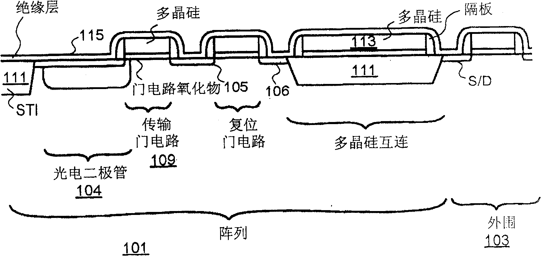
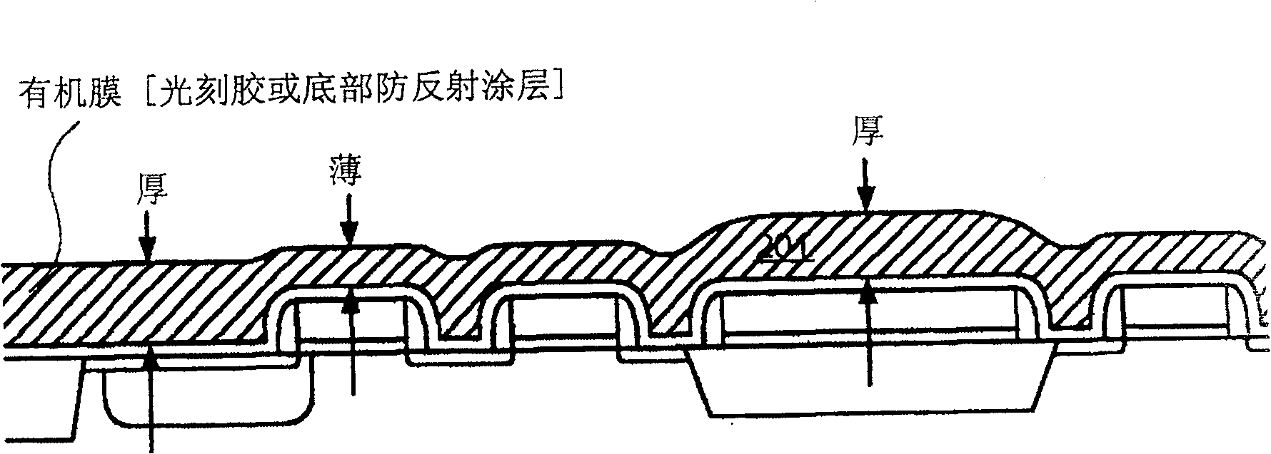
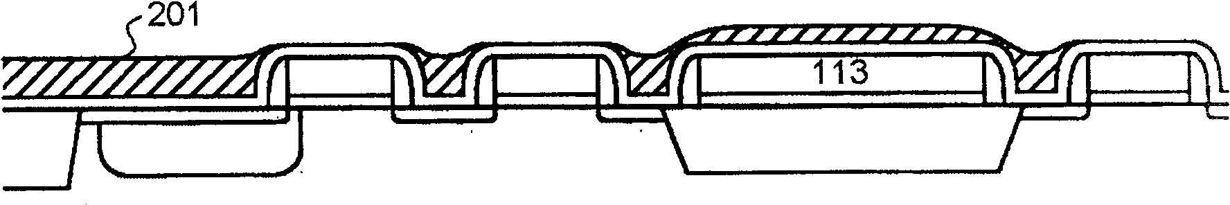
[0041] In the following description, numerous specific details are provided in order to provide a thorough understanding of specific embodiments of the invention. However, one skilled in the art will recognize that the invention can be practiced without one or more of these specific details, or that the invention can be practiced without other methods, elements, materials, operations, etc. . In addition, well-known structures and operations are not shown or described in detail in order to clearly describe the various embodiments of the present invention.

[0042] In the description of the present invention, when referring to "an embodiment" or "a certain embodiment", it means that the specific features, structures or characteristics described in this embodiment are included in at least one embodiment of the present invention. Thus, appearances of "in an embodiment" or "in a certain embodiment" in various places in the specification do not necessarily refer to all belonging to...


PUM


Abstract

A self-aligned silicide (salicide) process is used to form a silicide for a CMOS image sensor consistent with a conventional CMOS image sensor process flow. An insulator layer is deposited over the pixel array of the image sensor. An organic layer is deposited over the insulator layer. A chemical mechanical polish (CMP) is performed to remove the organic over raised polysilicon structures. Using the organic layer as a mask, portions of the insulator layer are removed and a metal layer is deposited. The metal layer is annealed to form a metal silicide.

Description

technical field [0001] The present invention relates to an image sensor, and more particularly, the present invention relates to an image sensor processed by a self-aligned metal silicide (salicide) process. Background technique [0002] Image sensors have become ubiquitous, and they are widely used in digital cameras, cellular phones, security cameras, medical equipment, automobiles, and other applications. The technology of manufacturing image sensors, especially CMOS (Complementary Metal Oxide Semiconductor) image sensors continues to develop rapidly. For example, the requirements of high resolution and low power consumption promote the further miniaturization and integration of image sensors. [0003] With further integration, an important feature of an image sensor is the ability to quickly read signals from the pixel array. Pixel arrays containing more than five million individual pixels are not uncommon. Many image sensors use a salicide process to improve the spee...

Claims


Application Information

Patent Timeline
Patent Type & Authority Patents(China)
IPC IPC(8): H01L21/82H01L21/3205
CPCH01L27/14806H01L27/14603H01L27/14643H01L27/14609
Inventor 霍华德·E·罗德斯
Owner OMNIVISION TECH INC
Why Eureka
Try Eureka