Method for making multi-step photodiode junction structure for backside illuminated sensor

A technology of image sensing device and manufacturing method, which is applied in radiation control devices, semiconductor/solid-state device manufacturing, electrical components, etc., can solve the problems of weakening the sensing ability of sensors, achieve the effect of increasing the sensitivity and improving the photosensitive characteristics

Active Publication Date: 2009-09-09
TAIWAN SEMICON MFG CO LTD
View PDF4 Cites 0 Cited by
  • Summary
  • Abstract
  • Description
  • Claims
  • Application Information

AI Technical Summary

Problems solved by technology

However, the thinned substrate may weaken the sensing ability of the sensor

Method used


Image

  • Method for making multi-step photodiode junction structure for backside illuminated sensor
  • Method for making multi-step photodiode junction structure for backside illuminated sensor
  • Method for making multi-step photodiode junction structure for backside illuminated sensor

Examples


Embodiment Construction

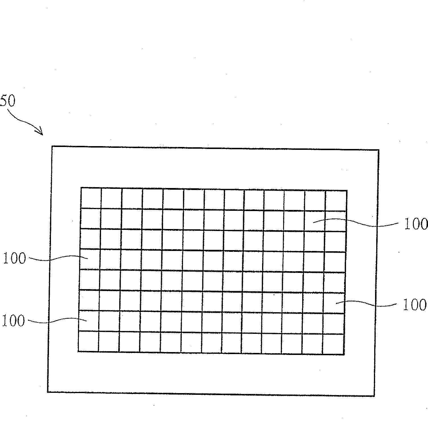
[0034] Please refer to figure 1 , which shows an image sensing device 50 composed of a plurality of back-illuminated pixels 100 forming a pixel array. In this embodiment, the pixel 100 may use components such as photosensitive diodes or photodiodes to record the intensity or brightness of light irradiated on the diodes. The image sensor device 50 may also use reset transistors, source follower transistors, pinned layer photodiodes, transfer transistors and other components. The image sensing device 50 may be a different type of image sensing device, such as a charge-coupled device (CCD), a complementary metal-oxide-semiconductor (CMOS) image sensing device, an active pixel sensing device (APS), or a passive pixel sensing device. device. The array formed by adjacent pixels 100 is usually provided with other circuits and output / input devices for pixel operation and communication with components other than pixels.

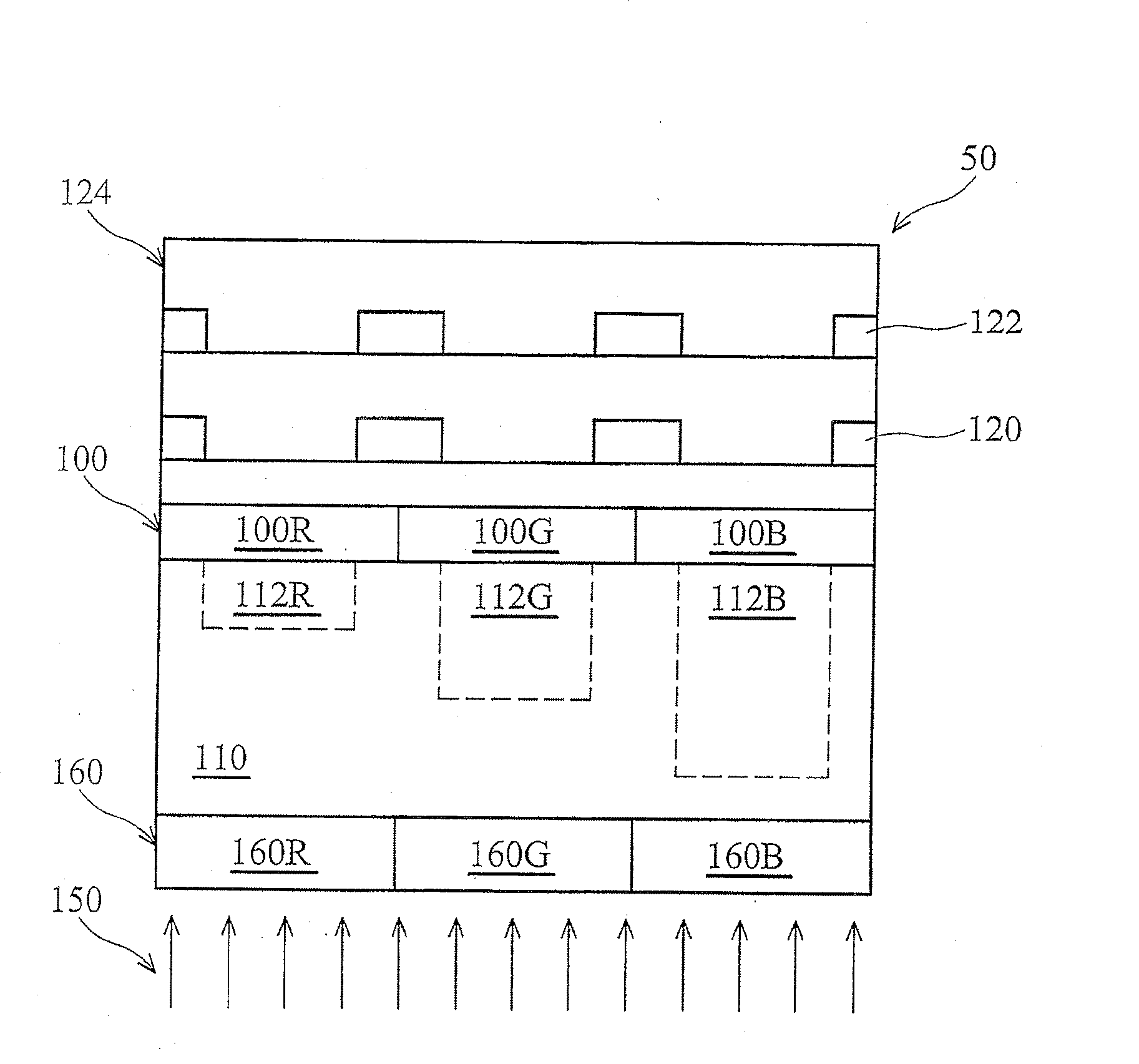
[0035] Please refer to figure 2 , the image sensing device ...


PUM


Abstract

The present invention provides a backlight image sensing device, comprising: a substrate; a first doped region located in the substrate; and a second doped region located in the substrate and above the first doped region, wherein The first doped region preferably reaches more than 50% of the thickness of the substrate. The present invention also provides a method for manufacturing a backlight image sensing device, comprising: preparing a substrate; performing a first ion implantation on the substrate to form a first doped region in the substrate; forming a polysilicon layer on the substrate and performing second ion implantation on the substrate to form a second doped region above the first doped region, wherein the first doped region is as deep as 50% or more of the thickness of the substrate. The invention can improve the photosensitive characteristics of the sensing device without affecting the performance of each component therein.

Description

technical field [0001] The present invention relates to a semiconductor device, and more particularly to a backlight image sensing device and a manufacturing method thereof. Background technique [0002] The image sensing device includes a pixel array (pixel array) composed of a plurality of photosensitive diodes or photodiodes, reset transistors, source follower transistors, fixed layer photoelectric Diodes (pinned layer photodiodes), and / or transfer transistors (transfer transistors) and other components used to record the light intensity on the diode. The above-mentioned pixel array generates electrons after sensing light, and the more light is sensed, the more electrons are generated. The electrons are then used by another circuit and thus produce the color and brightness suitable for a specific application such as a digital camera. Generally, the pixel array may be a charge-coupled device (CCD), or a complementary metal oxide semiconductor (CMOS) image sensing device....

Claims


Application Information

Patent Timeline
Patent Type & Authority Patents(China)
IPC IPC(8): H01L27/146H01L31/102H01L21/822H01L21/265H01L31/18
CPCH01L27/1464H01L27/14645
Inventor 许慈轩杨敦年
Owner TAIWAN SEMICON MFG CO LTD
Why Eureka
Try Eureka