Semiconductor laser device having incomplete bonding region and electronic equipment
A laser device and semiconductor technology, which is applied to the structure of semiconductor lasers, semiconductor devices, and optical waveguide semiconductors, can solve problems such as insufficient reliability improvement, achieve high reliability, suppress deformation, and improve reliability.
- Summary
- Abstract
- Description
- Claims
- Application Information
AI Technical Summary
Problems solved by technology
Method used
Image

Examples
no. 1 approach
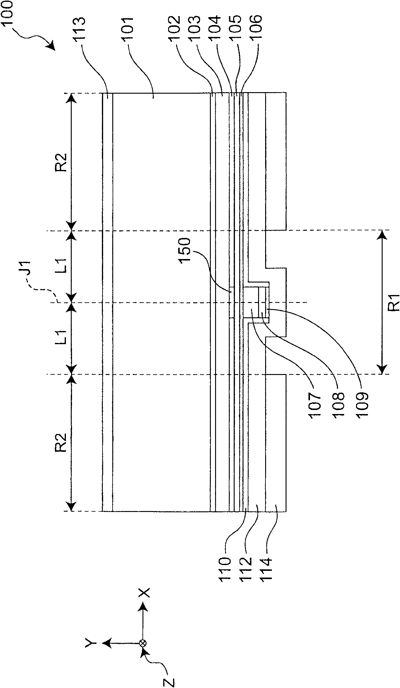
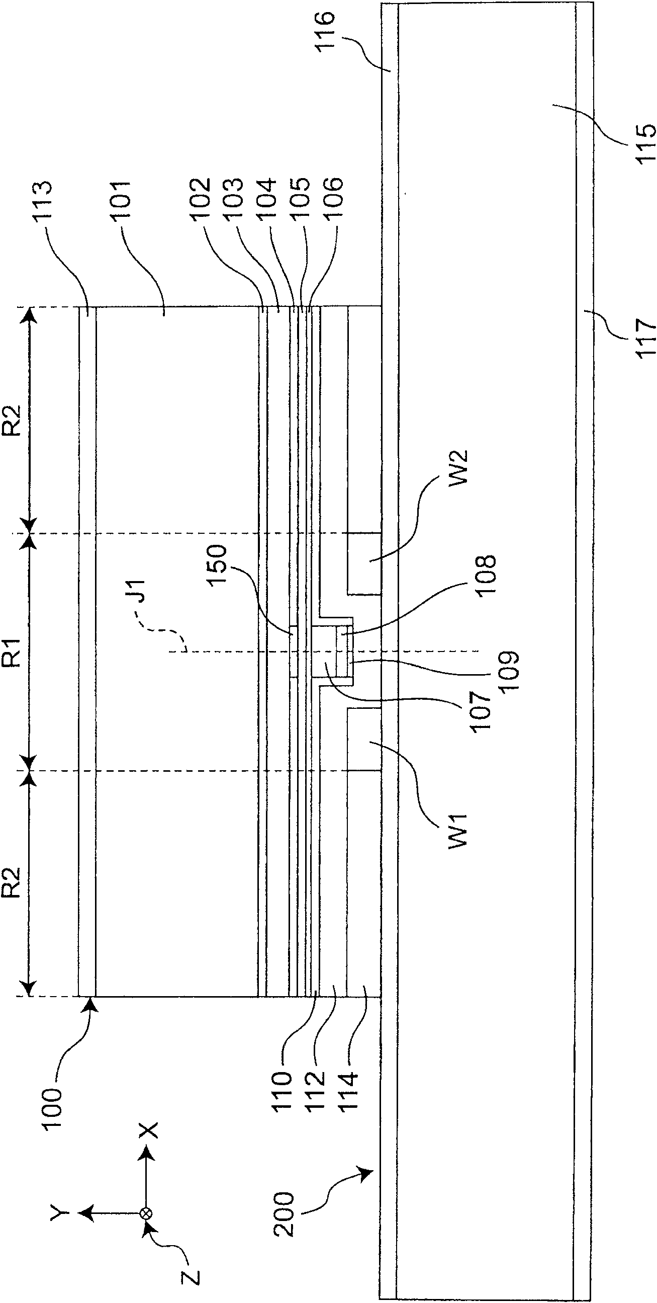
[0042] Figure 1AA cross section of the semiconductor laser element 100 included in the first embodiment of the semiconductor laser device of the present invention is shown. In this first embodiment, the semiconductor laser element 100 has a ridge structure. Semiconductor laser element 100 includes: n-GaAs substrate 101, n-GaInP buffer layer 102, n-AlGaInP cladding layer 103, quantum well active layer 104, p-AlGaInP first cladding layer 105, etch stop layer 106, p-AlGaInP The second cladding layer 107 , the p-GaAs contact layer 108 , the p-side contact electrode 109 , the dielectric film 110 , the plated metal layer 112 as a conductive electrode, and the n-electrode 113 .
[0043] In addition, the semiconductor laser element 100 has the Figure 1A The light-emitting area 150 extending in strips perpendicular to the direction of the paper. Furthermore, this semiconductor laser element 100 has a solder layer 114 laminated on the plated metal layer 112 .
[0044] The solder l...
no. 2 approach
[0061] figure 2 A second embodiment of the semiconductor laser device of the present invention is shown. This second embodiment, in place of Figure 1C The semiconductor laser element 100 differs from the first embodiment in that it has a semiconductor laser element 500 . Therefore, in this second embodiment, the same reference numerals are used for the same parts as those of the first embodiment, and differences from the first embodiment will be mainly described.
[0062] In the first embodiment, the second cladding 107 is left only in the region to become the ridge, and in the second embodiment, as figure 2 As shown, there is not only the second cladding layer 107 constituting the ridge, but also the second cladding layer TS separated from the second cladding layer 107 by a predetermined dimension (for example, 5 μm to 100 μm) on both sides in the X direction.
[0063] That is, in this second embodiment, at the time of manufacture, a region is etched from the end of the...
PUM
 Abstract
Description
Claims
Application Information
 - R&D
- Intellectual Property
- Life Sciences
- Materials
- Tech Scout
- Unparalleled Data Quality
- Higher Quality Content
- 60% Fewer Hallucinations
Browse by: Latest US Patents, China's latest patents, Technical Efficacy Thesaurus, Application Domain, Technology Topic, Popular Technical Reports.
© 2025 PatSnap. All rights reserved.Legal|Privacy policy|Modern Slavery Act Transparency Statement|Sitemap|About US| Contact US: help@patsnap.com