Method of preparing multistage silicon nano component

A technology of silicon nanometers and devices, which is applied in the field of preparing multilevel silicon nanometer devices, can solve the problems of limiting the application and development of multilevel devices, complex preparation steps, and slow processing speed, and achieve low cost, broad application prospects, and simple operation Effect

Inactive Publication Date: 2009-12-23
PEKING UNIV
View PDF4 Cites 0 Cited by
  • Summary
  • Abstract
  • Description
  • Claims
  • Application Information

AI Technical Summary

Problems solved by technology

These methods can realize the preparation of multi-level structures, and have the advantages of high resolution and accurate positioning; however, their common characteristics are that they all use expensive equipment and complicated preparation steps, and the processing speed is slow, which is Greatly limit the application and development of multi-level devices

Method used


Image

  • Method of preparing multistage silicon nano component
  • Method of preparing multistage silicon nano component
  • Method of preparing multistage silicon nano component

Examples


Embodiment 1

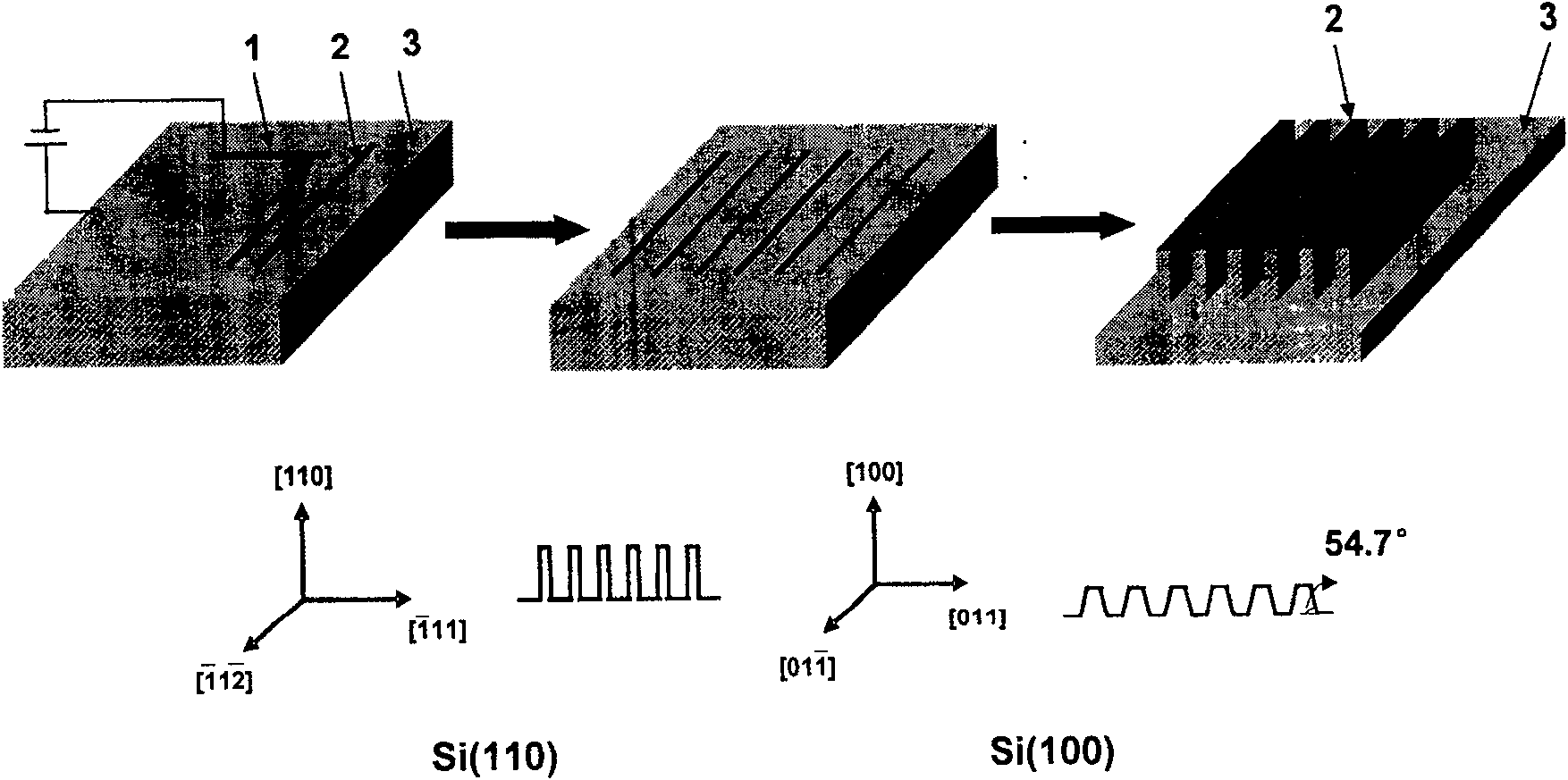
[0035] (1) Cut the commercially purchased Si(110) silicon wafer (Beijing Institute of Nonferrous Metals) into small pieces of 1cm×1cm, making one side parallel to the Si{111} crystal plane; , ultrasonic cleaning with deionized water for 3 minutes; use Piranha solution [concentrated H 2 SO 4 :H 2 o 2 =7:3 (volume ratio)] Treat the Si sheet at 90°C for 10 minutes, take it out and clean it with deionized water; treat the cleaned Si sheet with 1% (mass percent concentration) HF aqueous solution for 1 minute, and deionized Rinse with water; use high-purity N 2 blow dry.

[0036] (2) Put the Si sheet processed in step (1) on the sample stage of a commercial scanning probe microscope (SPM, Dimension3100, Digital Instrument Corporation), and the relative humidity of the environment is 60%; select the area to be processed, and design the corresponding pattern (a set of parallel lines) and set the tip path; apply a bias voltage (tip bias-6V, tip movement speed 40 μm / s) between the ...

Embodiment 2

[0040] (1) Select commercially purchased Si(100) silicon wafers (Beijing Institute of Nonferrous Metals), and the rest of the treatment is the same as the step (1) of Example 1.

[0041] (2) Except for the following specific conditions, other operations are the same as step (2) of Example 1: the relative humidity of the environment is 60%; the pattern is designed as a group of squares; the needle tip bias is -6V, and the needle tip movement speed is 1 micron / second.

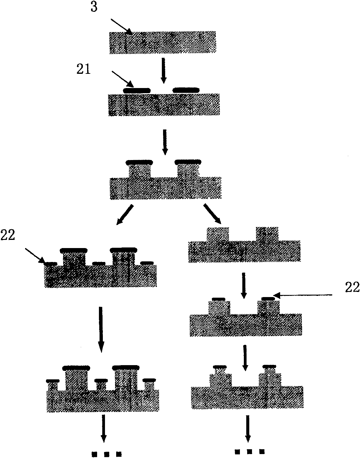
[0042] (3) Put the sample treated in step (2) into the prepared wet etching solution [20% KOH aqueous solution, 50°C], and the control time is 120s; quickly take it out and put it in deionized water, wash, blow Dry.

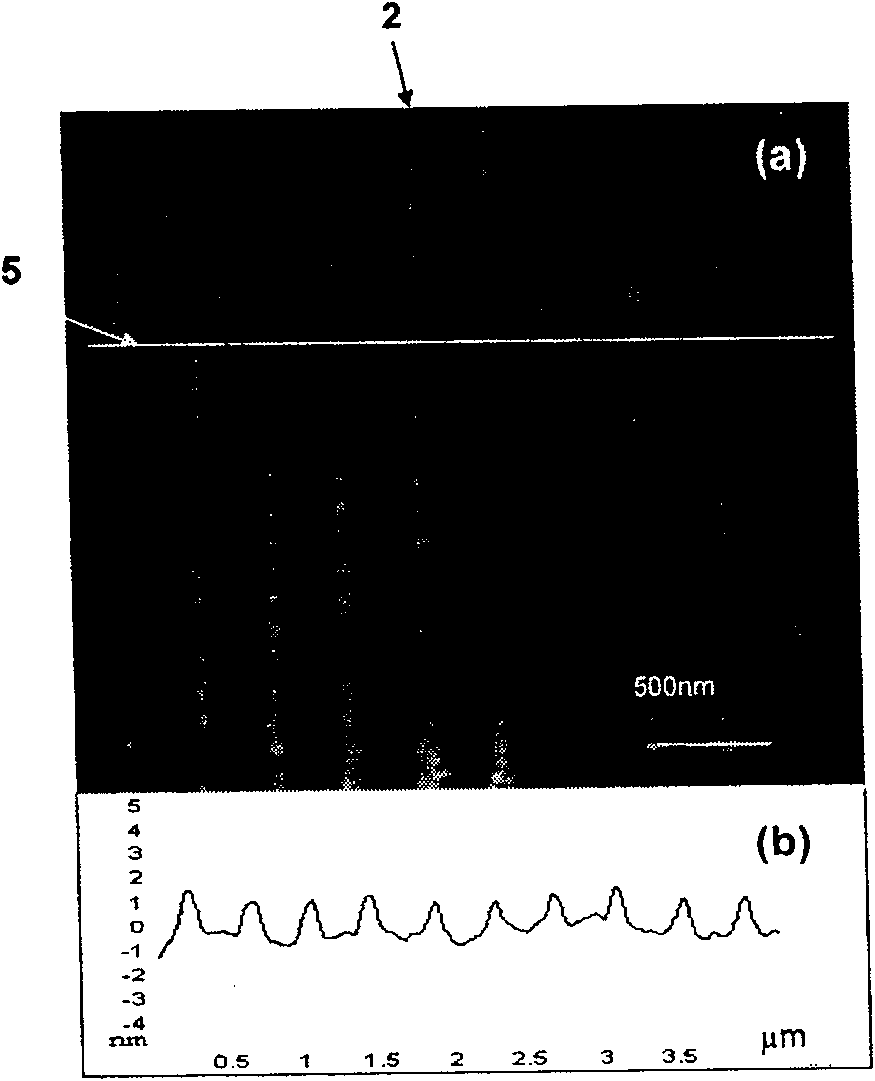
[0043] (4) Scanning and imaging the processed structure with a scanning probe microscope (SPM, Dimension3100) again. As a result, an inverted pyramid structure was obtained as shown in Fig. 4(b), the width of the top line was 79.0nm, the width of the bottom line was 176.2nm, with inclined side wall...

Embodiment 3

[0045] (1) with the step (1) of embodiment 2

[0046] (2) except the following specific conditions, all the other operations are with the step (2) of implementation example 1: 40% of the relative humidity of the environment; the designed pattern is a combined pattern (a group of parallel lines, a group of periods is a grid of 1 micron, a A group of square grids with a period of 500nm, a group of diamond-shaped grids with a side length of 1 micron); the tip bias voltage is -12V, and the tip movement speed is 10 microns / second.

[0047] (3) Put the sample treated in step (2) into the prepared wet etching solution [20% KOH aqueous solution, 50°C], and the control time is 30s; quickly take it out and put it in deionized water, wash, blow Dry.

[0048] (4) Scanning and imaging the processed structure with a scanning probe microscope (SPM, Dimension3100) again. The result is shown in Figure 4(c), and the following combined patterns are obtained: a group of parallel lines, a group ...


PUM

PropertyMeasurementUnit
heightaaaaaaaaaa
widthaaaaaaaaaa

Abstract

The invention discloses a method for preparing a multilevel silicon nanometer device. The method comprises at least one cycle of the following steps: 1) using a scanning probe microscope to carry out scanning probe oxidation on the Si-H surface to be processed on the silicon substrate to obtain a nanoscale oxide pattern; 2) performing step 1) to obtain The silicon chip with the oxide pattern is placed in an anisotropic etching solution for reaction to obtain the required multi-level silicon nanometer element. The method for preparing multilevel silicon nano-devices of the present invention combines the advantages of high resolution and flexible operation of the scanning probe microscope and the relatively mature chemical wet etching technology (anisotropic wet etching technology) in the microelectronics industry , to achieve the preparation and processing of multi-level nanostructures. The method has high resolution, strong controllability, low cost, and simple operation, which provides a flexible and convenient way for the processing and preparation of multilevel nano-devices, and has broad application prospects in the field of nano-devices.

Description

technical field [0001] The invention relates to a method for preparing a multilevel silicon nanometer device. Background technique [0002] The invention and application of integrated circuits based on silicon devices has brought about the ever-changing information age and profound changes in the production and life of human society. On the one hand, the increase in device integration requires the development of devices from planar combinations to multi-level complex types; on the other hand, multi-level structures have potential applications in many fields, such as micro / nano electromechanical devices, fluid devices, optical devices, etc. , which makes the preparation and processing of multi-level structures attract more and more attention. [0003] At present, there are several methods to realize the preparation and processing of multi-level structures in the submicron scale, such as electron beam lithography (EBL), X-ray lithography (XRL), focused ion beam lithography (F...

Claims


Application Information

Patent Timeline
Patent Type & Authority Patents(China)
IPC IPC(8): B82B3/00H01L21/00H01L21/30H01L21/205
Inventor 张锦张莹莹刘忠范罗刚
Owner PEKING UNIV
Why Eureka
Try Eureka