

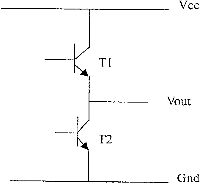
Technique for preparing bipolar type long-direction NPN tube using phosphorus-buried and deep phosphorus-buried technique
A bipolar, deep phosphorous technology, used in semiconductor/solid-state device manufacturing, electrical components, circuits, etc., can solve the problems of high antimony buried layer resistance, affecting the output power of power amplifier circuits, and small antimony diffusion coefficient.
- Summary
- Abstract
- Description
- Claims
- Application Information
AI Technical Summary
Problems solved by technology
Method used
Image

Examples
specific Embodiment approach
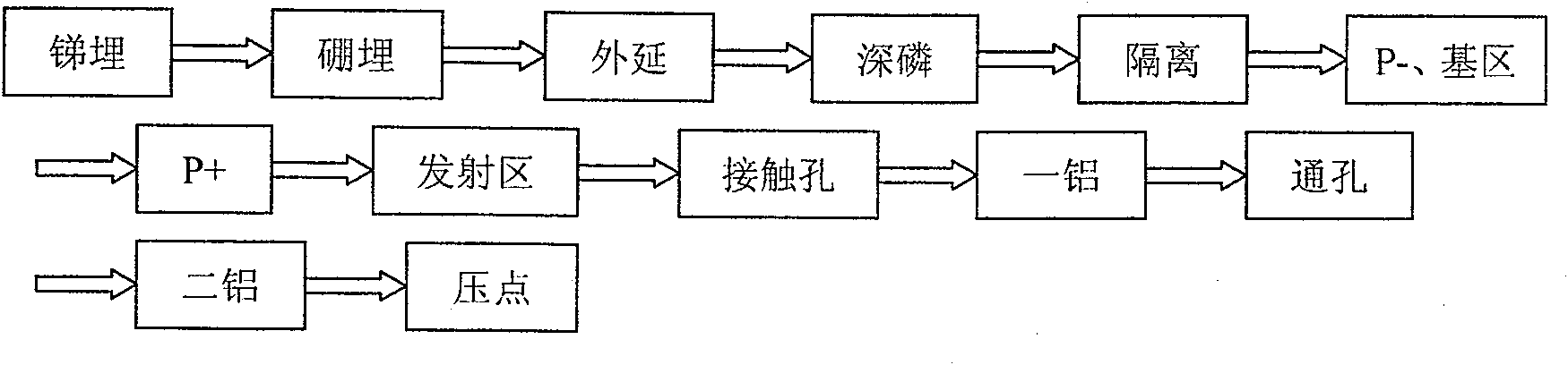
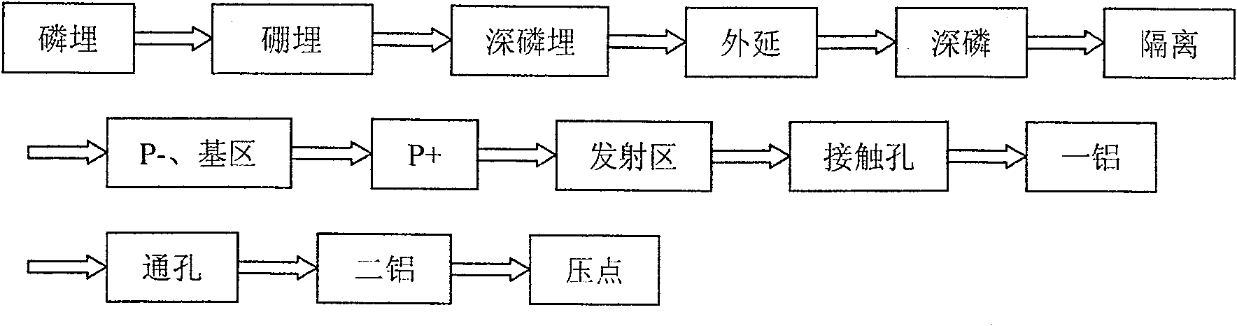
[0058] The specific implementation of the bipolar process using phosphorus buried and deep phosphorus buried technology is as follows:
[0059] 1. Feeding: P type, crystal orientation ,
[0060] 2. Oxidation: Thickness
[0061] 3. Phosphorus buried photolithography and corrosion; engrave the vertical NPN tube N buried area window,
[0062] 4. Phosphorus buried implantation: the implantation energy is 80KeV, and the implantation dose is 1E15; the impurity is phosphorus, and the N-buried area of the NPN tube is injected with phosphorus,
[0063] 5. Phosphorus buried annealing: the annealing condition is 1200°C for 300 minutes N2+120 minutes O2,
[0064] 6. Boron buried photolithography and implantation: the implantation area is the isolation trench area, the implantation energy is 80KeV, the implantation dose is 5E14, and the impurity is boron.
[0065] 7. Deep phosphorus buried lithography and implantation: the implantation area is a deep phosphorus area, the implantatio...
PUM
 Abstract
Description
Claims
Application Information