

Production method for polysilicon grid of DRAM
A technology of polysilicon gate and manufacturing method, which is applied in semiconductor/solid-state device manufacturing, electrical components, semiconductor devices, etc., can solve problems such as word line and bit line short circuit, and achieve the effect of solving short circuit and solving prominent problems
- Summary
- Abstract
- Description
- Claims
- Application Information
AI Technical Summary
Problems solved by technology
Method used
Image

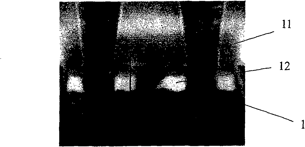
Examples
Embodiment 1
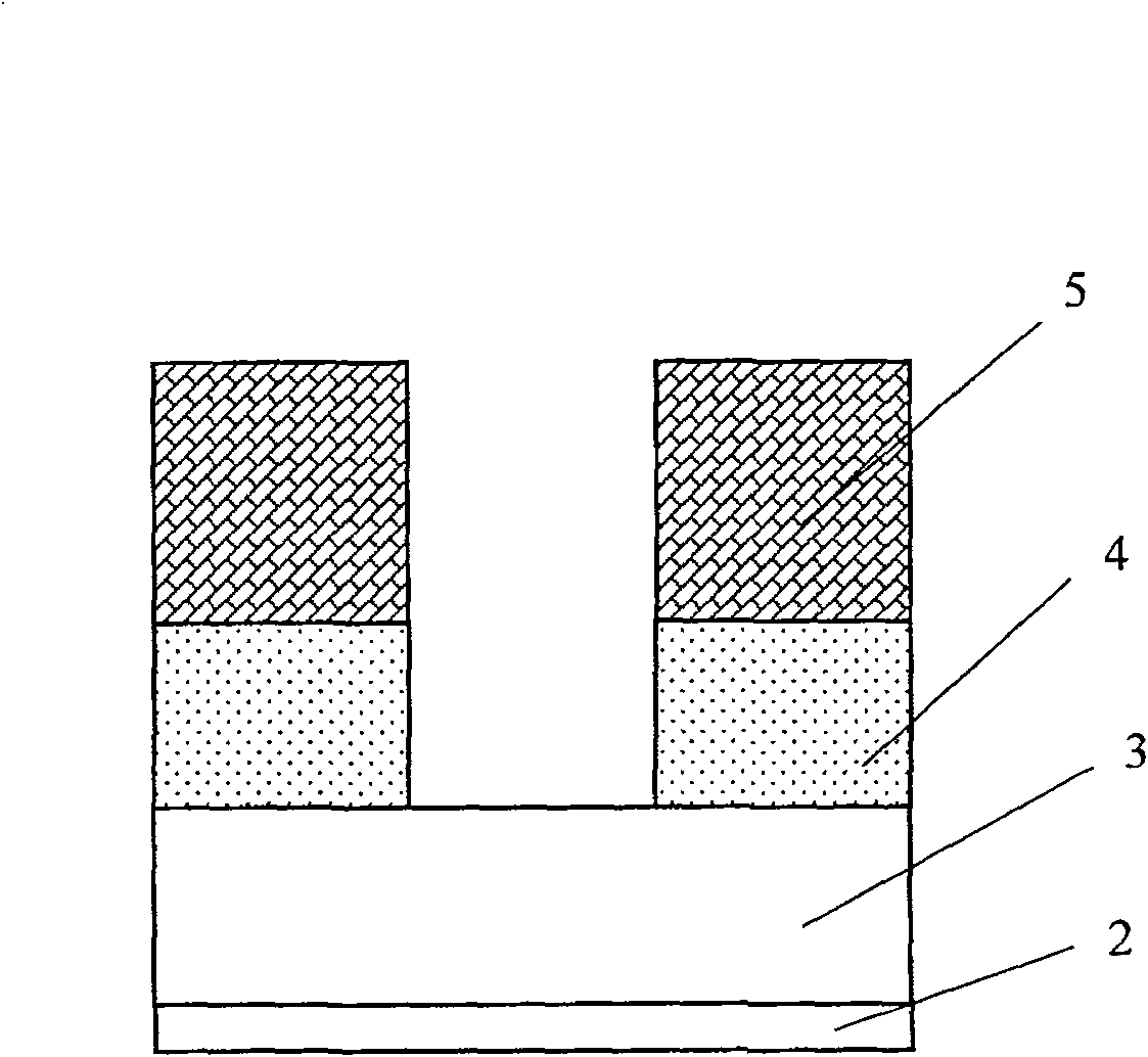
[0048] Figure 3a~3c It is a schematic diagram of the fabrication process of the polysilicon gate according to an embodiment of the present invention. Wherein, firstly, the gate silicon oxide layer 22 is formed by thermally growing silicon oxide on the silicon substrate, with a thickness of 4.0-8.0 nanometers. The thermally grown silicon oxide used is a conventional method and will not be described in detail here.
[0049] Then, the polysilicon layer 23 is deposited and formed by using conventional techniques, such as chemical vapor deposition, with a thickness of 60-100 nanometers.
[0050] Forming the tungsten silicide (WSix) layer 24 on the polysilicon layer can adopt conventional techniques, such as on the polysilicon layer, first depositing tungsten with chemical vapor deposition, and then heating to make tungsten and polysilicon at high temperature, such as 565 ℃, under pressure Under 1.2 Torr, react for 45 seconds to form tungsten silicide with a thickness of 80-120 n...
Embodiment 2
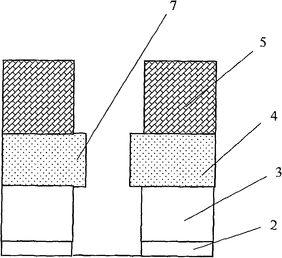
[0059] Figures 4a-4e It is a schematic diagram of the fabrication process of the polysilicon gate according to another embodiment of the present invention.
[0060] Wherein, firstly, the gate silicon oxide layer 22 is formed by thermally growing silicon oxide on the silicon substrate, with a thickness of 4.0-8.0 nanometers. The thermally grown silicon oxide used is a conventional method and will not be described in detail here.
[0061] Then, the polysilicon layer 23 is deposited and formed by using conventional techniques, such as chemical vapor deposition, with a thickness of 60-100 nanometers.
[0062] To form the WSix layer 24 on the polysilicon layer, conventional techniques can be used, such as first depositing tungsten on the polysilicon layer by chemical vapor deposition, and then heating to make the tungsten and polysilicon react at a high temperature, such as 565° C. and a pressure of 1.2 Torr, for 45 seconds. , forming tungsten silicide, the thickness of which is...
PUM
| Property | Measurement | Unit |
|---|---|---|
| depth | aaaaa | aaaaa |
| thickness | aaaaa | aaaaa |
| thickness | aaaaa | aaaaa |
Abstract
Description
Claims
Application Information