Green light LED
A light-emitting diode and green light technology, which is applied in semiconductor devices, electrical components, circuits, etc., can solve the problems of poor antistatic ability, low external quantum efficiency, and low external quantum efficiency of green light-emitting diodes, so as to reduce V-type defects , Strong antistatic ability
- Summary
- Abstract
- Description
- Claims
- Application Information
AI Technical Summary
Problems solved by technology
Method used
Image
Examples
Embodiment 1
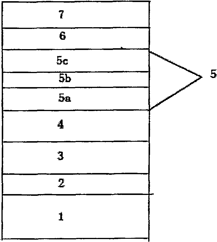
[0023] Using MOCVD equipment to epitaxially grow high-brightness green light-emitting diodes, the substrate used is (001) sapphire. Such as figure 1 As shown, firstly, the sapphire substrate 1 was heated to 1200 °C in the MOCVD reaction chamber, under H 2 The temperature is lowered for 5 minutes, and then the temperature is lowered to 500-600°C to grow a GaN nucleation layer 2 with a thickness of about 30nm; then the temperature is raised to 1160°C, and the H 2 As a carrier gas, epitaxially grow a 4-micron thick GaN buffer layer at a growth rate of 3.0 microns / hour, including a 0.5-micron thick unintentionally doped GaN layer 3 and a 3.5 micron-thick Si-doped n-type GaN buffer layer 4, The doping concentration of silicon is 5×10 17 cm -3 up to 5×10 19 cm -3 between; then lower the temperature to 650-750°C, switch the carrier gas to N 2 , grow 5 In on this buffer layer 0.2 Ga 0.8 N(2.5nm) / In 0.8 Ga 0.2 N(0.5nm) / GaN(10nm), where the molar flow of TEGa is 0.1×10 -5 mol...
Embodiment 2
[0025] Using MOCVD equipment to epitaxially grow high-brightness green light-emitting diodes, the substrate used is (001) sapphire. Such as figure 1 As shown, firstly, the sapphire substrate 1 was heated to 1200 °C in the MOCVD reaction chamber, under H 2 The temperature is lowered for 5 minutes, and then the temperature is lowered to 500-600°C to grow a GaN nucleation layer 2 with a thickness of about 30nm; then the temperature is raised to 1160°C, and the H 2 As a carrier gas, epitaxially grow a 4-micron thick GaN buffer layer at a growth rate of 3.0 microns / hour, including a 0.5-micron thick unintentionally doped GaN layer 3 and a 3.5 micron-thick Si-doped n-type GaN buffer layer 4, The doping concentration of silicon is 5×10 17 cm -3 up to 5×10 19 cm -3 between; then lower the temperature to 650-750°C, switch the carrier gas to N 2 , grow 5 In on this buffer layer 0.2 Ga 0.8 N(2.5nm) / Al 0.8 Ga 0.2 N(0.5nm) / GaN(10nm), where the molar flow of TEGa is 0.1×10 -5mol / ...
PUM
| Property | Measurement | Unit |
|---|---|---|
| thickness | aaaaa | aaaaa |
Abstract
Description
Claims
Application Information

