

Method for optimizing route for exposing wafer
A path optimization and path technology, applied in the field of photolithography, can solve the problems of long exposure time, consumption, affecting the system exposure yield, etc., and achieve the effect of shortening the consumption time and improving the yield.
- Summary
- Abstract
- Description
- Claims
- Application Information
AI Technical Summary
Problems solved by technology
Method used
Image

Examples
Embodiment Construction
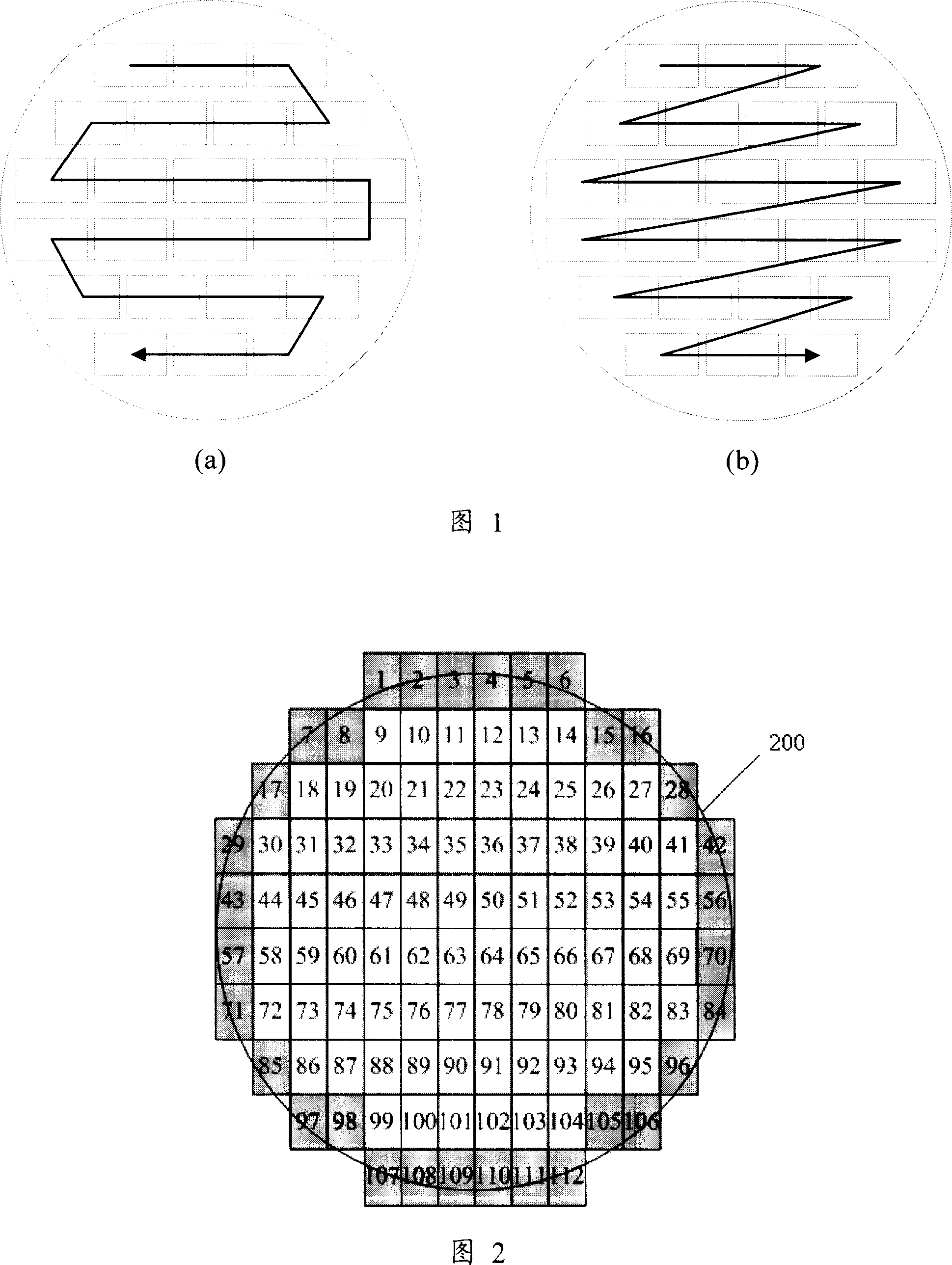
[0025] The method for optimizing the wafer exposure path of the present invention will be summarized below.
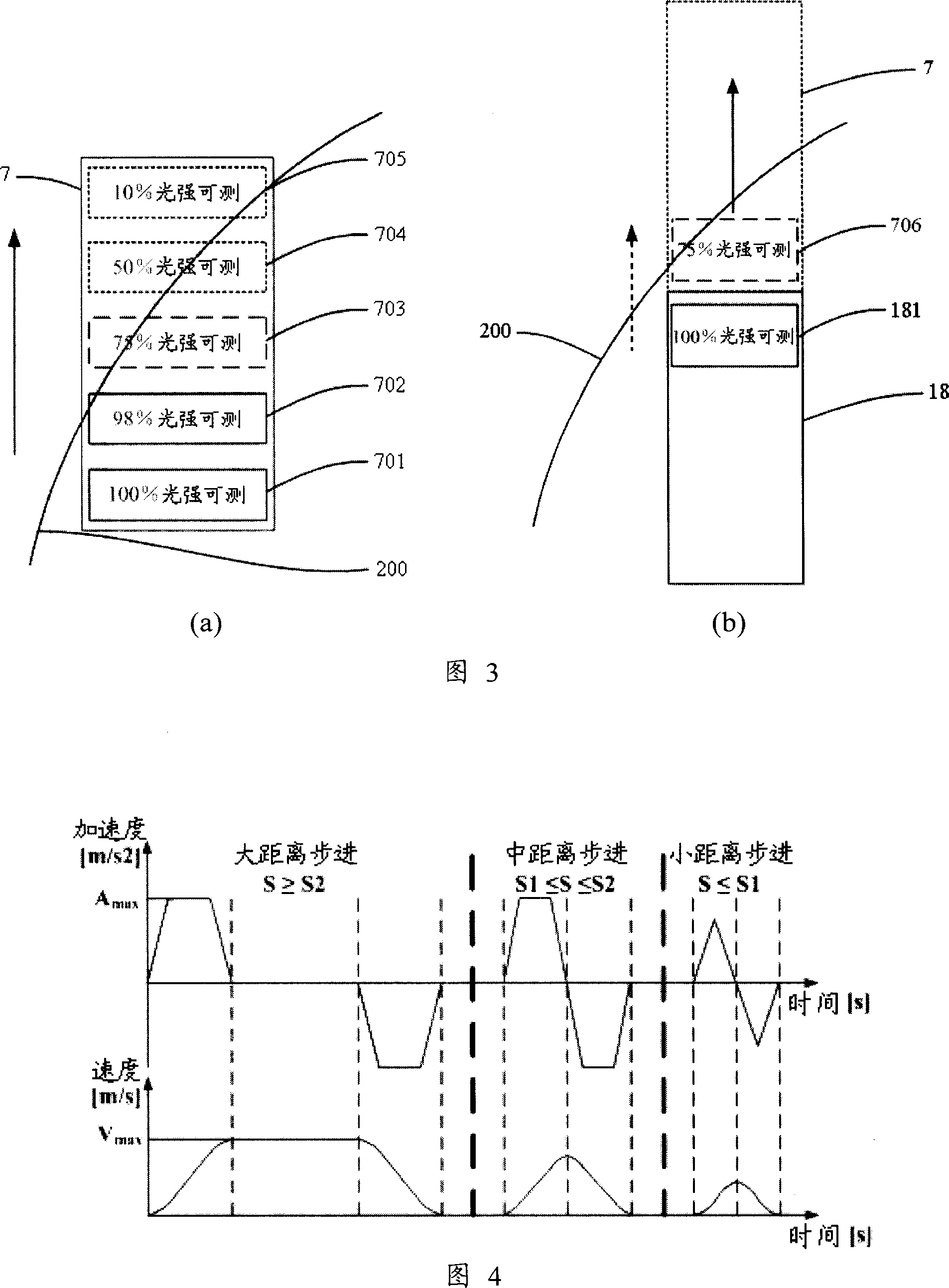
[0026] First, it is necessary to determine the exposure field distribution and exposure path constraints. The exposure field distribution is determined according to the process parameters of the product with the assistance of the lithography machine process software. The exposure field distribution information mainly includes the center coordinates of each exposure field and the state to be exposed. The purpose of collecting the exposure field distribution information is to Further determine the limitation conditions of the exposure path, and provide reference data for subsequent steps such as scanning and exposure. Exposure path constraints are used to judge the legitimacy of an exposure path, which mainly depends on the measurability of the leveling parameters of the exposure field. Referring to Fig. 2, it has shown the exposure field distribution of a kind of wafer...
PUM
 Abstract
Description
Claims
Application Information