

Wiring board
A wiring board and substrate technology, applied in the direction of multilayer circuit manufacturing, printed circuit components, electrical components, etc.
- Summary
- Abstract
- Description
- Claims
- Application Information
AI Technical Summary
Problems solved by technology
Method used
Image

Examples
Embodiment approach 1
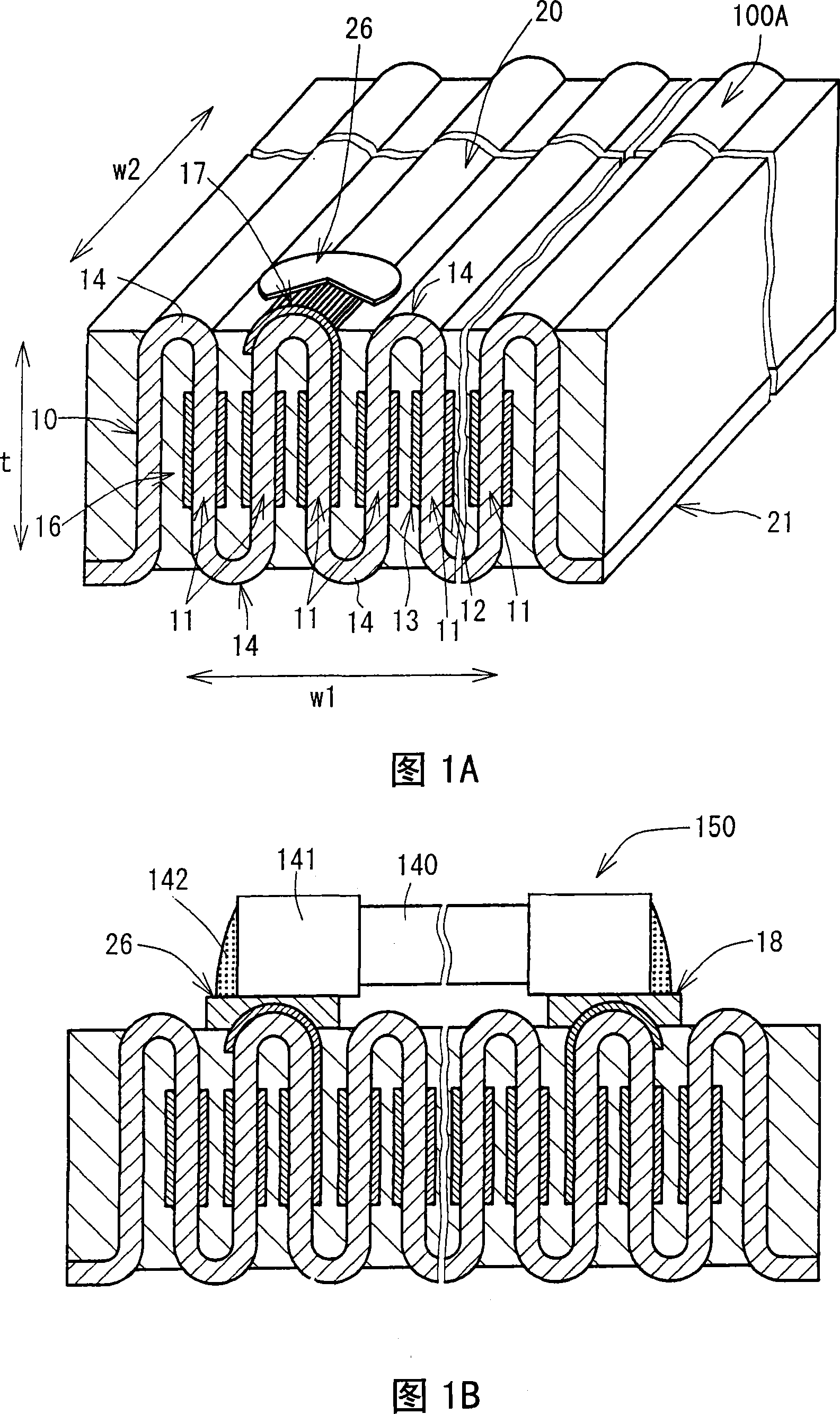
[0204] FIG. 1A shows a substrate structure of a wiring board 100A according to a preferred embodiment 1 of the present invention. A wiring board 100A shown in FIG. 1A has a shape of a rectangular flat plate. Wiring board 100A includes a plurality of dielectric layers 11 . The respective dielectric layers 11 are arranged along the direction in which the main surfaces of the substrates face each other (thickness direction), and are stacked in the direction w1 crossing the facing direction t at right angles. The orthogonal direction w1 refers to the planar direction of the substrate along either side of the rectangular wiring board 100A. Internal conductor patterns 12 and 13 are provided on the respective dielectric layers 11 . Each internal conductor pattern 12 and 13 is provided on both surfaces of each dielectric layer 11 . On one of the main surfaces 20 and 21 of the substrate, adjacent dielectric layers 11 are formed to be connected to each other so as to be integrally co...
Embodiment approach 2
[0226] 4A, 4B, 4C and 5 show the structure of a wiring board 100B according to the preferred embodiment 2 of the present invention and its manufacturing method. The configurations of the dielectric layer 11, the internal conductor patterns 12 and 13, and the lead-out electrodes 17 are similar to those of the preferred embodiment 1. However, in the present preferred embodiment, the extraction electrode 17 is provided on one main surface 20 of the wiring board 100B, and the extraction electrode 19 is provided on the other main surface 21 of the wiring board 100B. The lead electrodes 17 and 19 are connected through the internal conductor patterns 12 and 13 on the upper and lower surfaces of the wiring board 100B.
[0227] In order to mount chip-type circuit components such as LSI chips at high density, circuit components (electronic parts, etc.) are provided on both surfaces of the wiring board, and must be mounted on one of the surfaces of the wiring board The circuit component...
Embodiment approach 3
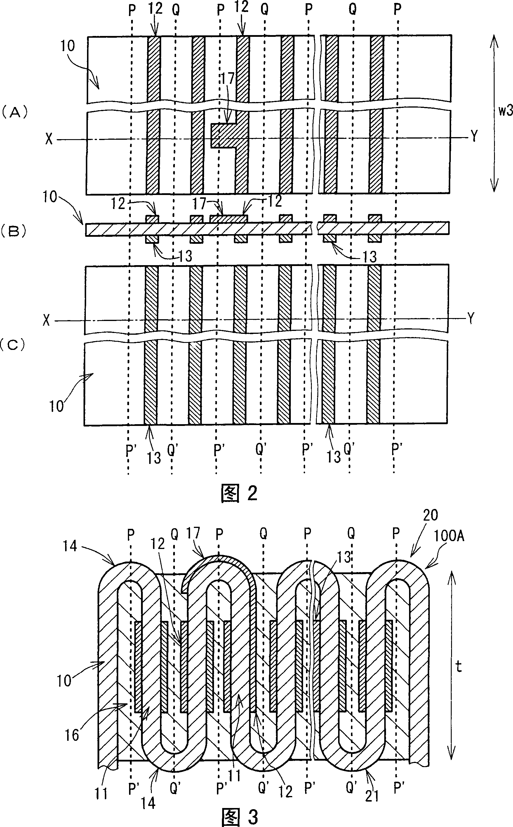
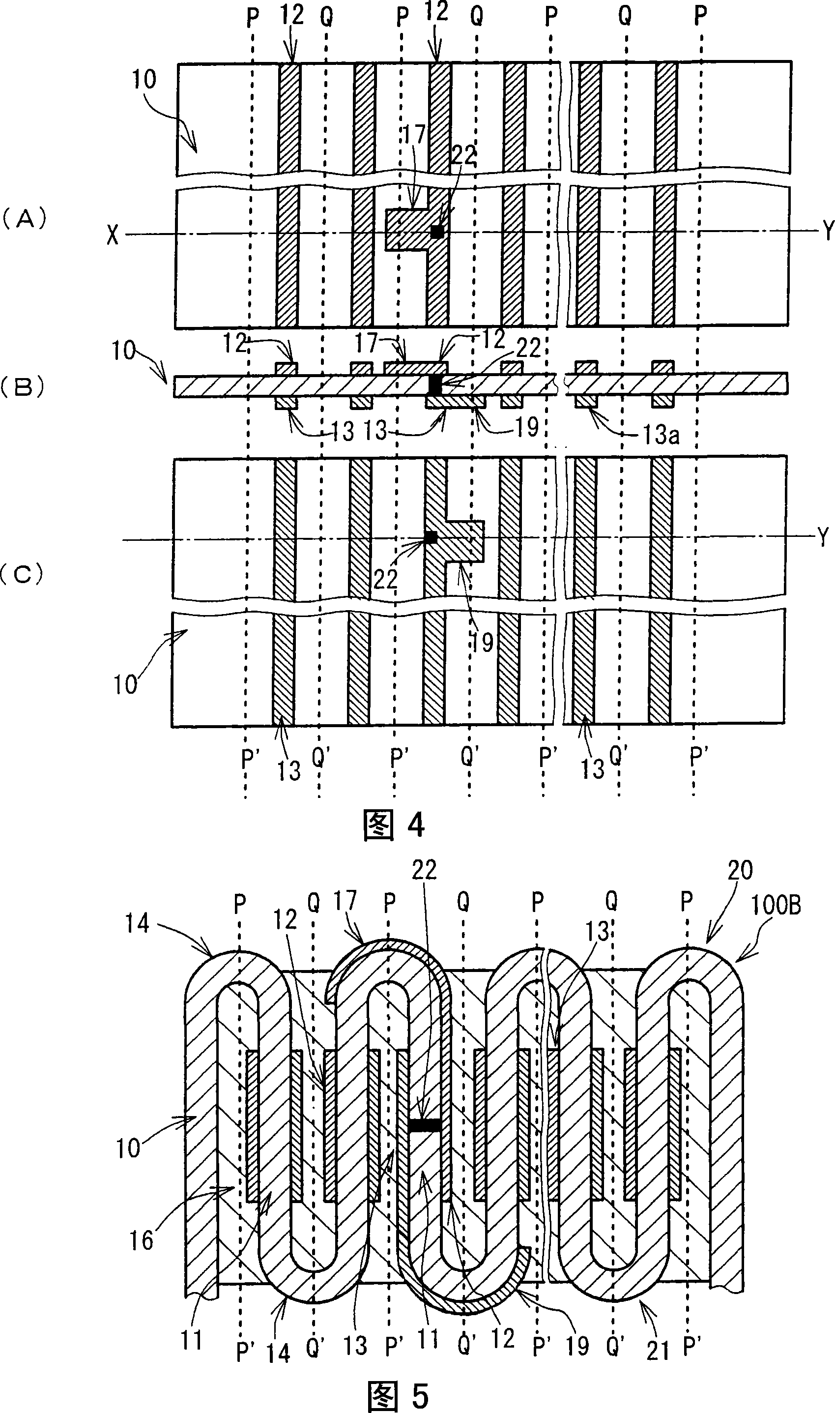
[0241] 8A, 8B, 8C, 9 and 10 show the configuration of a wiring board 100C according to a preferred embodiment 3 of the present invention. The basic structure according to this preferred embodiment is the same as that of the preferred embodiment 1. The present preferred embodiment is characterized in that different inner conductor patterns 12 are connected to each other.
[0242] The basic constitution according to the present invention is characterized in that internal conductor patterns formed at high density are incorporated in the wiring board. The individual internal conductor patterns formed parallel to each other in the planar direction of the dielectric layer cannot be connected to each other in the wiring board.
[0243] It is also conceivable that the signal lines connecting the inner conductor pattern constituting one signal line with the inner conductor pattern constituting the other signal line are hard-wired. Figures 8A, 8B, 8C, 9 and 10 show the configuration o...
PUM
| Property | Measurement | Unit |
|---|---|---|
| Thickness | aaaaa | aaaaa |
| Width | aaaaa | aaaaa |
| Thickness | aaaaa | aaaaa |
Abstract
Description
Claims
Application Information