Residue removing method after circuit board laser drill processing

A technology of laser drilling and circuit boards, which is applied in the field of drilling processing, can solve problems such as lack of fit, affect the stability of laser processing, and inconvenience, and achieve the effect of improving efficacy

Inactive Publication Date: 2007-08-15
COMPEQ MFG
View PDF0 Cites 0 Cited by
  • Summary
  • Abstract
  • Description
  • Claims
  • Application Information

AI Technical Summary

Problems solved by technology

[0003] As far as the currently used drilling processing method is concerned, please refer to Fig. 5 and Fig. 6, wherein the circuit board 40 is covered with metal copper skin 41 on the upper and lower surfaces of the non-conductive plate, and the perforated hole is to be set. The position is drilled by drilling 42 technology, for example: using laser drilling, so when the drilling 42 is performed, the cut copper slag will be splashed on the copper skin 41, which will affect the subsequent The production of the circuit may affect the correctness of the circuit; moreover, the fluff formed on the surface of the copper surface of the multi-layer circuit board after blackening treatment, if it is not properly protected during drilling , will affect the processing stability of it

Method used


Image

  • Residue removing method after circuit board laser drill processing
  • Residue removing method after circuit board laser drill processing
  • Residue removing method after circuit board laser drill processing

Examples


Embodiment Construction

[0027] In order to further explain the technical means and effects that the present invention takes to achieve the intended purpose of the invention, the specific implementation of the method for removing residues after laser drilling of circuit boards proposed according to the present invention will be described below in conjunction with the accompanying drawings and preferred embodiments. , method, step, feature and effect thereof, detailed description is as follows.

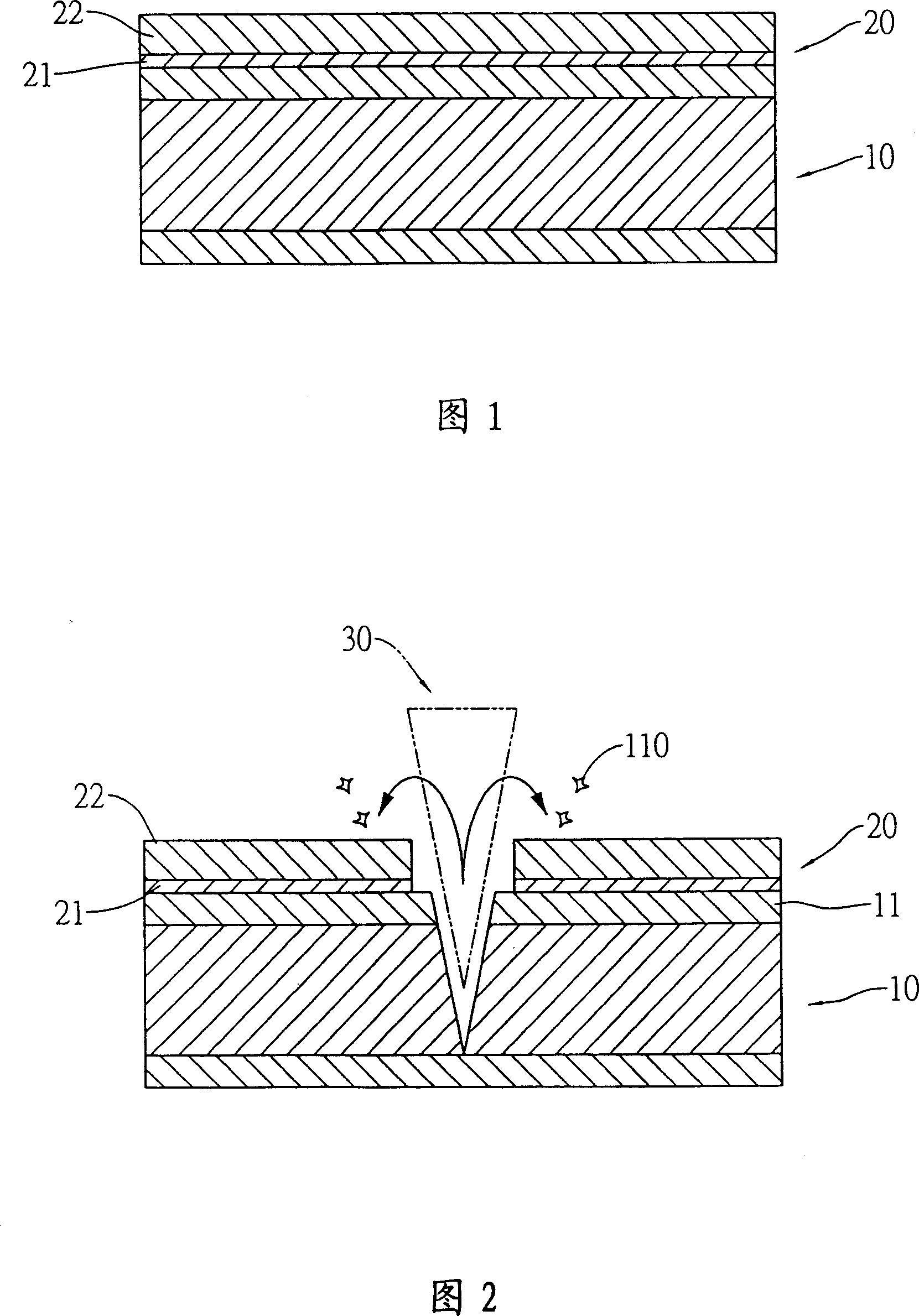
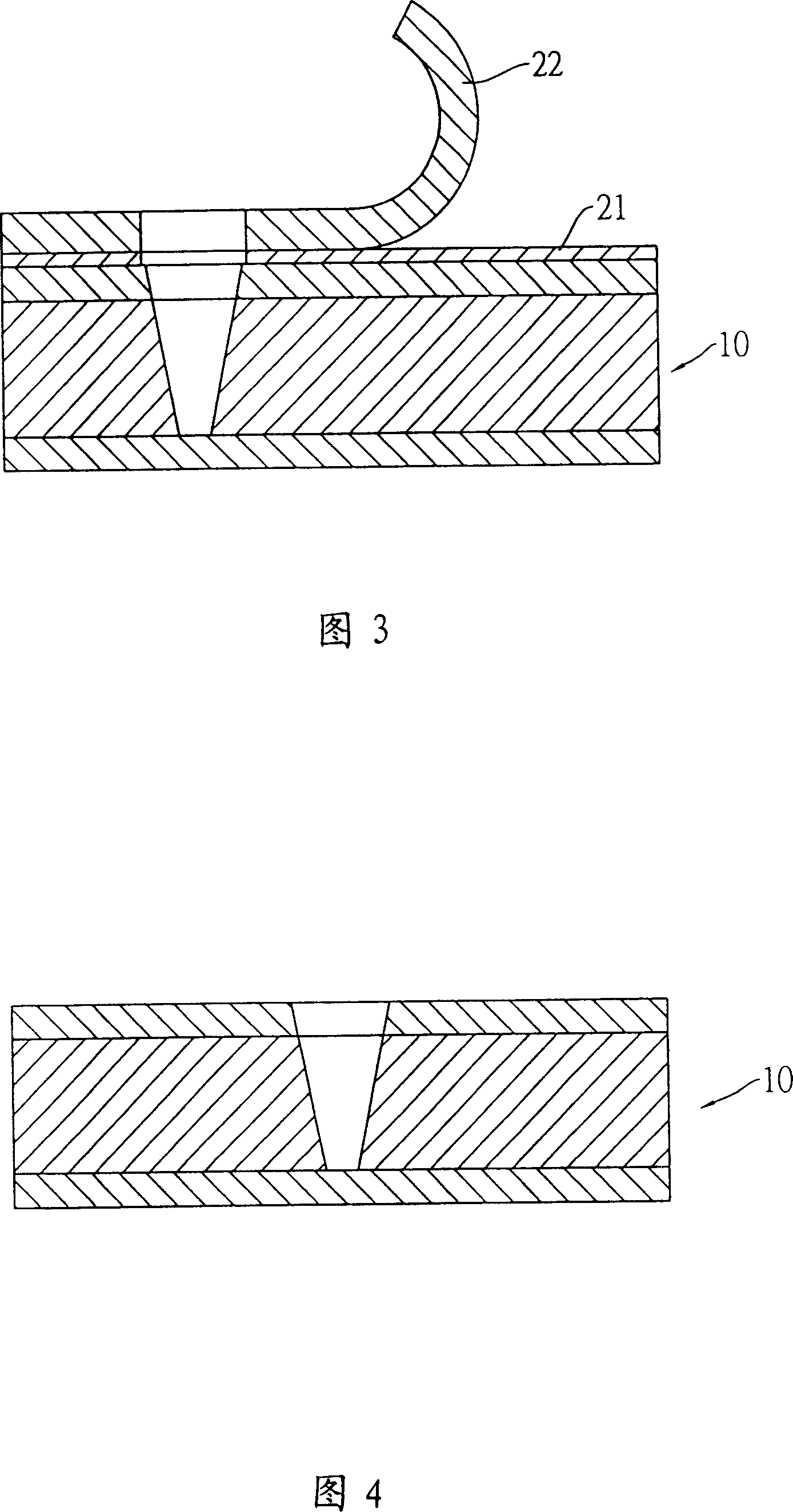
[0028] Please refer to FIG. 1 , the method for removing residue after laser drilling of a circuit board according to a preferred embodiment of the present invention, wherein the circuit board 10 is coated with copper skins 11 on the upper surface and the lower surface of the non-conductive plate, respectively, A dry film 20 is coated on the copper skin 11 to be formed, and the dry film 20 is formed by sequentially coating a photoresist layer 21 and a PET film 22 .

[0029] After the copper skin 11 has been bla...


PUM


Abstract

The invention relates to a slag removing method of circuit board laser drilling hole, which coats dry membrane on the circuit board, and drills, therefore, the generated copper slag is above dry membrane, and the dry membrane can be removed after drilling to remove the copper slag.

Description

technical field [0001] The invention relates to a drilling method, in particular to a method for removing residues after laser drilling of circuit boards, in particular to a method for protecting circuit boards after processing and providing circuit boards after completion. Background technique [0002] In the production of circuit boards in the prior art, in addition to forming circuits on the circuit board, perforations must also be provided on the circuit board to provide plug-in installation of various electronic components, or to provide them as circuit boards. It is used for the conduction of the circuit between the upper layer and the lower layer. Therefore, drilling the circuit board, especially the processing and application of the circuit board of the multi-layer board, is indeed an extremely important and necessary process. [0003] As far as the currently used drilling processing method is concerned, please refer to Fig. 5 and Fig. 6, wherein the circuit board 40...

Claims


Application Information

Patent Timeline
IPC IPC(8): B23K26/18B23K26/38B23K26/382
Inventor 杨伟雄林澄源吕俊贤
Owner COMPEQ MFG
Why Eureka
Try Eureka