Design method for on-chip spiral inductor with the wearing metal conductor line width and gap

A technology of metal conductors and spiral inductors, which is applied in the direction of inductors, semiconductor devices, fixed inductors, etc., can solve the problems of inductance quality factor Q value decrease, increase, inner diameter decrease, etc., to achieve the decrease of series equivalent resistance, preparation The effect of process compatibility and low energy loss

Inactive Publication Date: 2007-08-15
SHANGHAI INTEGRATED CIRCUIT RES & DEV CENT +1
View PDF0 Cites 17 Cited by
  • Summary
  • Abstract
  • Description
  • Claims
  • Application Information

AI Technical Summary

Problems solved by technology

The smaller the spacing, the stronger the magnetic field interaction, which will lead to a more uneven current density in the metal conductor, making the metal conductor series resistance R s In addition, when the other parameters of the inductance remain unchanged, if the distance between the two metal conductors becomes larger, the total length of the metal conductors will become larger and the inner diameter will become smaller, which is also will make the metal conductor series resistance R s further increases, thereby also affecting the quality factor Q value of the inductance to decrease

Method used


Image

  • Design method for on-chip spiral inductor with the wearing metal conductor line width and gap

Examples


Embodiment Construction

[0024] The design method of the on-chip spiral inductor with graded metal conductor line width and spacing of the present invention will be further described in detail below.

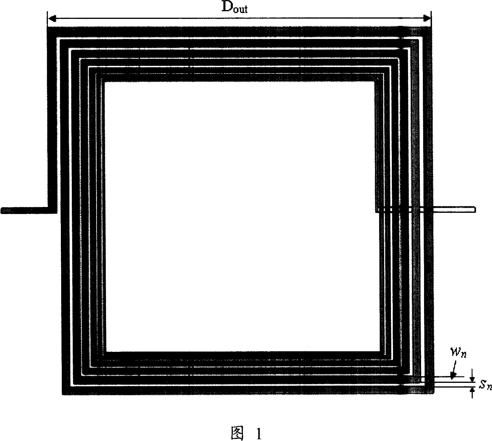
[0025] The on-chip spiral inductor to be designed by the present invention includes a substrate and a metal conductor coil formed on the substrate with a gradually changing metal conductor line width and spacing. The line width gradually increases, and the distance between two adjacent turns of metal conductors also gradually increases. Assume that the number of turns of the metal conductor coil is N, and the numbers from the inner circle to the outer circle are 1, 2, ..., N, and w n (n=1, 2,..., N) represents the line width of any circle of metal conductor, with s n (n=1, 2,..., N-1) represents the distance between any two adjacent circles of metal conductors, then w n and s n The value of satisfies the following formula:

[0026] When N is an odd number, w N +w 1 =w N-1 +w 2 =w N-2 +w 3 =......


PUM

PropertyMeasurementUnit
widthaaaaaaaaaa
widthaaaaaaaaaa
widthaaaaaaaaaa

Abstract

The invention provides a design method for chip spiral inductor with gradual-change metal conductor linewidth and span. Wherein, it calculates the linewidth wn and nearby conductor span sn by following formula: for odd N, wN+w1=wN-1+w2=...=2w(N+1)/2=2w, sN-1+s1=sN-2+s2 =...=s(N+1)/2+s(N-1)/2=2s; for even N, wN+w1=wN-1+w2=...=w(N/2)+1+wN/2=2w, sN-1+s1= sN-2+s2=...=2sN/2=2s; and wn+1>wn, sn+1>sn. This invention reduces vortex effect and near effect generated by spiral inductor at HF to decreases serial equivalent resistance and energy loss.

Description

technical field [0001] The invention relates to integrated circuit manufacturing technology, in particular to a design method for on-chip spiral inductors of integrated circuit chips. Background technique [0002] In the development of CMOS radio frequency integrated circuits (RFICs), the most urgent and difficult thing is to produce high-performance new devices and new unit circuits, which are the basis for realizing monolithic CMOS integrated RF front-ends. As a key component in radio frequency integrated circuits, on-chip spiral inductors are widely used in various modules of the radio frequency front end, such as radio frequency preselection loops, low noise amplifiers (LNAs), voltage controlled oscillators (VCOs), and LC loops. It is also the most difficult component to design and master in the circuit, and its performance parameters directly affect the performance of radio frequency integrated circuits. On-chip spiral inductors can realize the integration of inductors...

Claims


Application Information

Patent Timeline
Patent Type & Authority Applications(China)
IPC IPC(8): H01L27/00H01L27/02H01L23/522H01F17/00H01F37/00
Inventor 王勇石艳玲陈寿面赵宇航
Owner SHANGHAI INTEGRATED CIRCUIT RES & DEV CENT
Why Eureka
Try Eureka