A method for making MEMS switch, and MEM device and its making method

An electromechanical device and device technology, which is applied to the manufacture of microelectromechanical system switches and the field of microelectromechanical devices and their manufacture, can solve the problems of scrapped switches and unsatisfactory contact points, and achieve the effects of high yield and lower industrial costs.

Inactive Publication Date: 2007-08-15
周嘉兴
View PDF1 Cites 26 Cited by
  • Summary
  • Abstract
  • Description
  • Claims
  • Application Information

AI Technical Summary

Problems solved by technology

For example, if the dimples are made too shallow then the contact point will not be ideal
In the worst case, if the dimple is made too deep, a connection will form between the dimple and the input transmission line, rendering the switch useless

Method used


Image

  • A method for making MEMS switch, and MEM device and its making method
  • A method for making MEMS switch, and MEM device and its making method
  • A method for making MEMS switch, and MEM device and its making method

Examples


Embodiment Construction

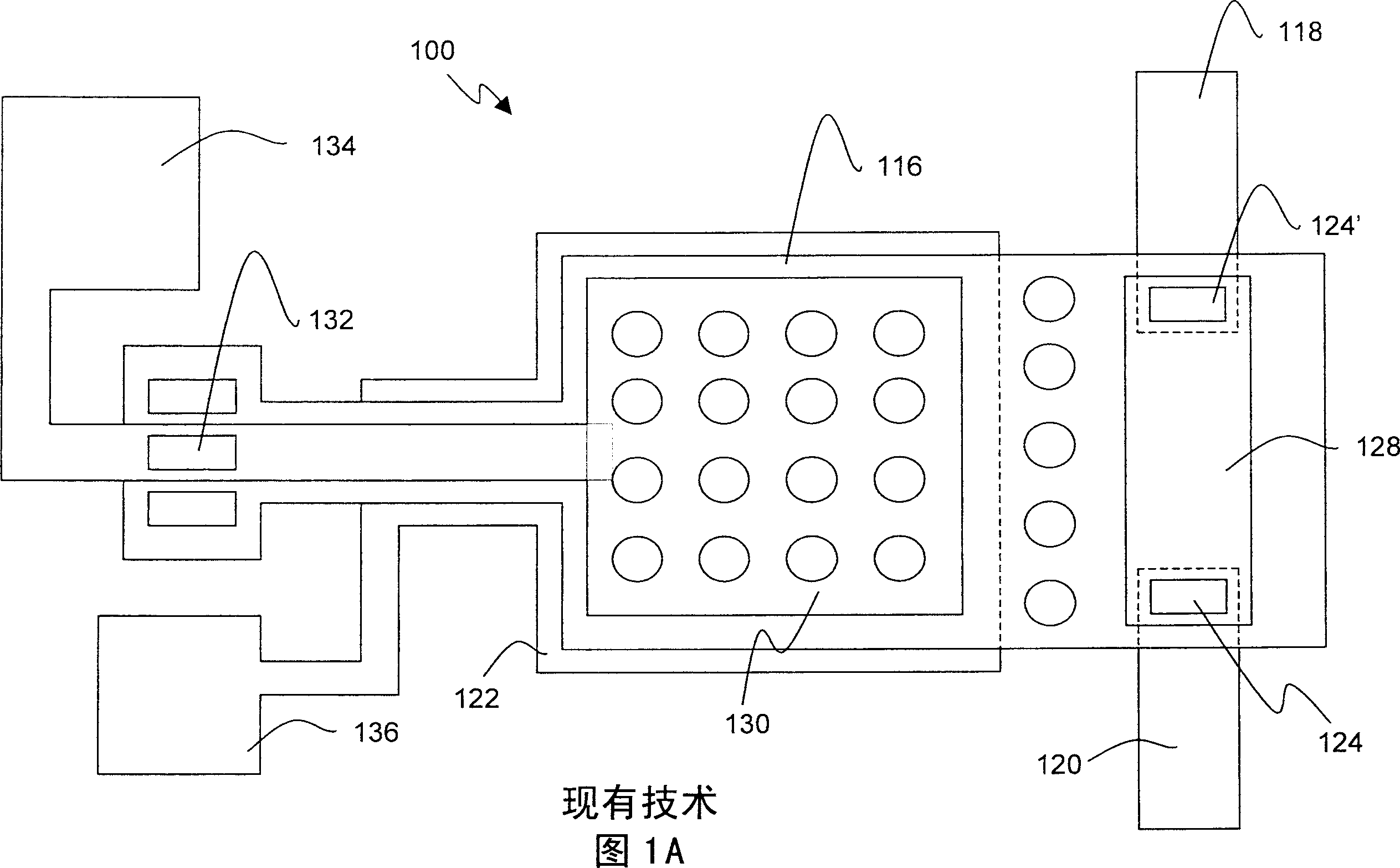
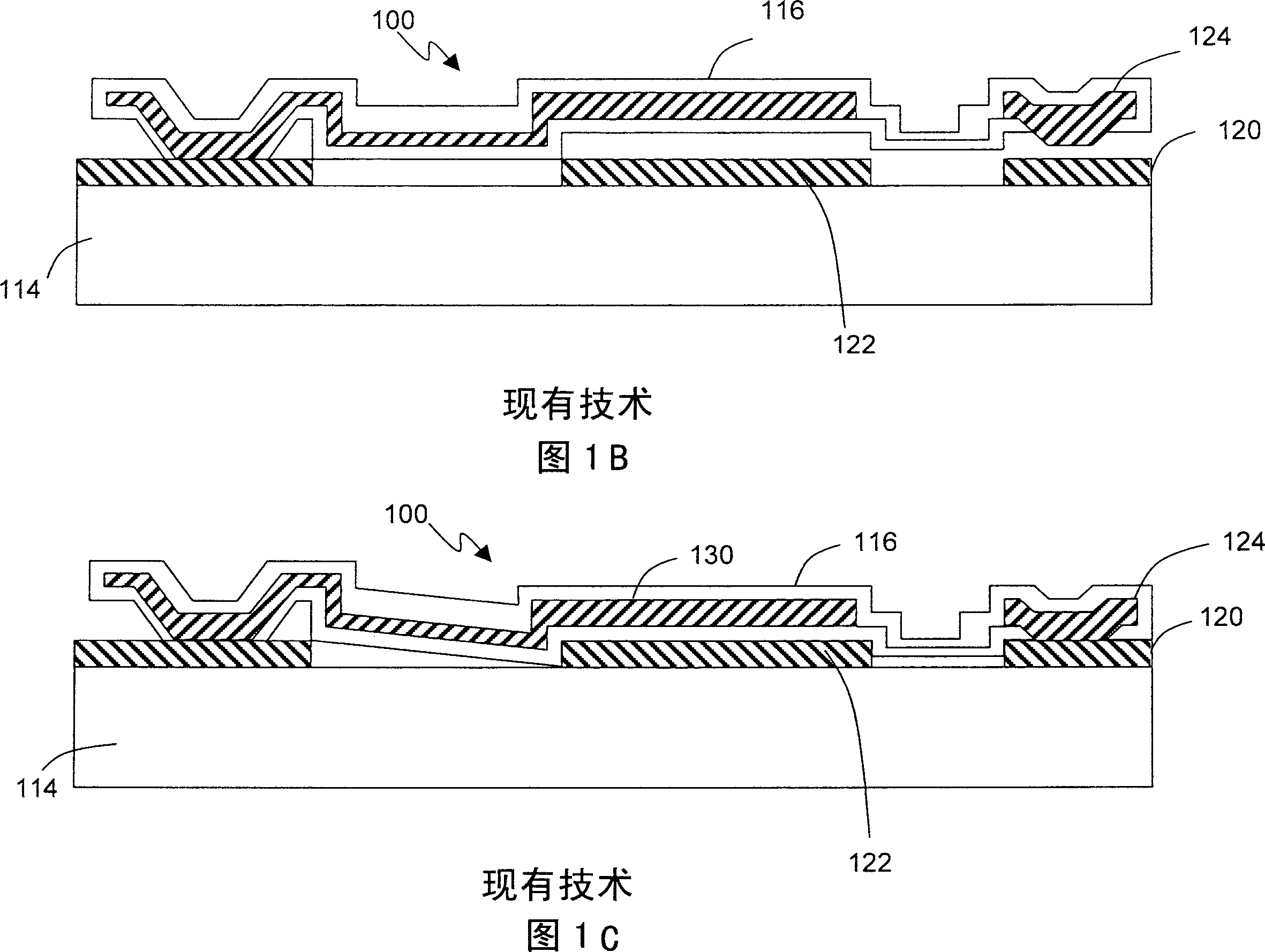
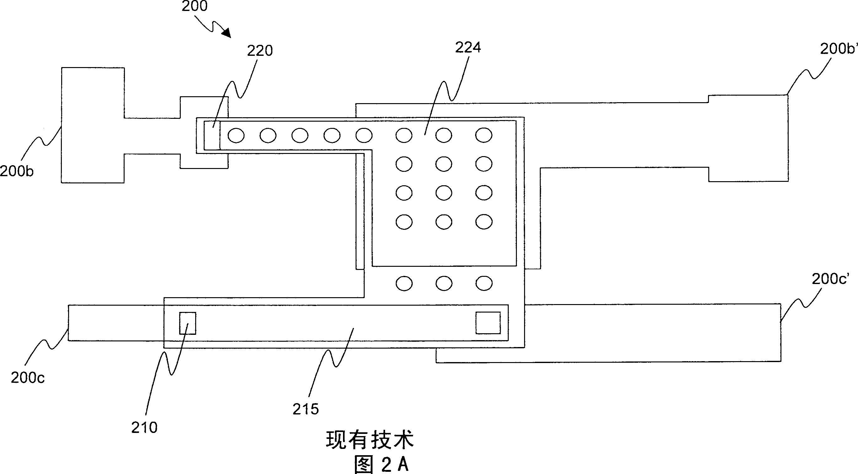
[0075] The invention relates to a production technology for improving the reliability and performance of a microelectromechanical system (MEMS) switch contact point. Specifically, the present invention relates to a planarization process for a cantilever beam, surface passivation of a substrate, and a unique design of metal dimples for making reproducible and durable contact points, as well as a method for making a common A ground plane layer and a set of contact teeth for MEMS technology. The following description, in conjunction with the accompanying drawings, enables one of ordinary skill in the art to make and use the invention and to use it in conjunction with the detailed application. Various modifications (such as use in different applications) will become apparent to those skilled in the art and apply to a wide range. The invention is therefore not limited to the aspects described, but is to be accorded the widest scope consistent with the principles and novel features...


PUM

PropertyMeasurementUnit
thicknessaaaaaaaaaa
thicknessaaaaaaaaaa

Abstract

A method for pseudo-planarization of an electromechanical device and for forming a durable metal contact on the electromechanical device and devices formed by the method are presented. Two principal aspects of the method include the formation of a planarized dielectric/conductor layer on a substrate and the formation of an electrode in an armature of a microelectromechanical switch, with the electrode formed such that it interlocks a structural layer of the armature to ensure it remains fixed to the armature over a large number of cycles. The present invention also relates to a system and method for making MEM switches having a common ground plane. One method for making MEM switches includes: patterning a common ground plane layer on a substrate; forming a dielectric layer on the common ground plane layer; depositing a DC electrode region through the dielectric layer to contact the common ground plane layer; and depositing a conducting layer on the DC electrode region so that regions of the conducting layer contact the DC electrode region, so that the common ground plane layer provides a common ground for the regions of the conducting layer.

Description

technical field [0001] The present invention relates to the production technology that can improve the reliability, yield and performance of the contact point of the micro-electro-mechanical system (MEMS, micro-electro-mechanical system) micro-relay switch. Specifically, the present invention relates to a planarization of a cantilever beam process, surface passivation of substrates, and unique design of metal dimples to make contacts with reproducible and durable contacts, and a method for producing microelectromechanical devices with a common ground plane layer and a set of contact teeth piece of technology. Background technique [0002] Currently, there are two types of MEMS used in radio frequency (RF) and microwave fields, one is a capacitive film switch called a shunt switch, and the other is a metal contact switch called a series switch. In addition to the above two types, the design can also be changed depending on the method of switch actuation. In general, switche...

Claims


Application Information

Patent Timeline
Patent Type & Authority Applications(China)
IPC IPC(8): B81B3/00H01H1/00B81C1/00B44C1/22C03C15/00C03C25/68C23F1/00H01H51/22H01H57/00H01H59/00H01L21/00H01L31/00H01P1/10
CPCY10T29/49105B81C1/00611B81C2201/0121H01H2059/0072H01H59/0009B81B3/00H01H11/00
Inventor 周嘉兴
Owner 周嘉兴
Why Eureka
Try Eureka