Laminated varistor and producing method thereof

A technology of varistor and manufacturing method, applied in resistance manufacturing, varistor, resistor, etc., can solve problems such as poor solvent resistance, and achieve enhanced thermal shock resistance, improved mechanical properties, resistance consistency and resistance. Excellent solvent properties

Inactive Publication Date: 2007-08-22
SHANGHAI CHANGYUAN WAYON CIRCUIT PROTECTION CO LTD
View PDF2 Cites 0 Cited by
  • Summary
  • Abstract
  • Description
  • Claims
  • Application Information

AI Technical Summary

Problems solved by technology

U.S. Patent No. 5658833 illustrates a method of manufacturing such a surface-mounted varistor. A varistor film is painted on an insulating layer, then covered with an insulating layer, and finally covered on the upper and lower insulating layers. A cover layer of another composition, so that a thin film varistor with good mechanical properties is obtained; the base material of some traditional surface mount varistors is a polymer material, which is used in US Patent No.5790587 The FR-4 epoxy board is used as the substrate, and copper is used as the electrode. After a series of processes such as copper cladding, etching, UV curing, and laser resistance adjustment, the resistance of the varistor obtained in this way is very consistent. However, due to the high polymer material its own limitations, its poor solvent resistance

Method used


Image

  • Laminated varistor and producing method thereof
  • Laminated varistor and producing method thereof
  • Laminated varistor and producing method thereof

Examples


Embodiment Construction

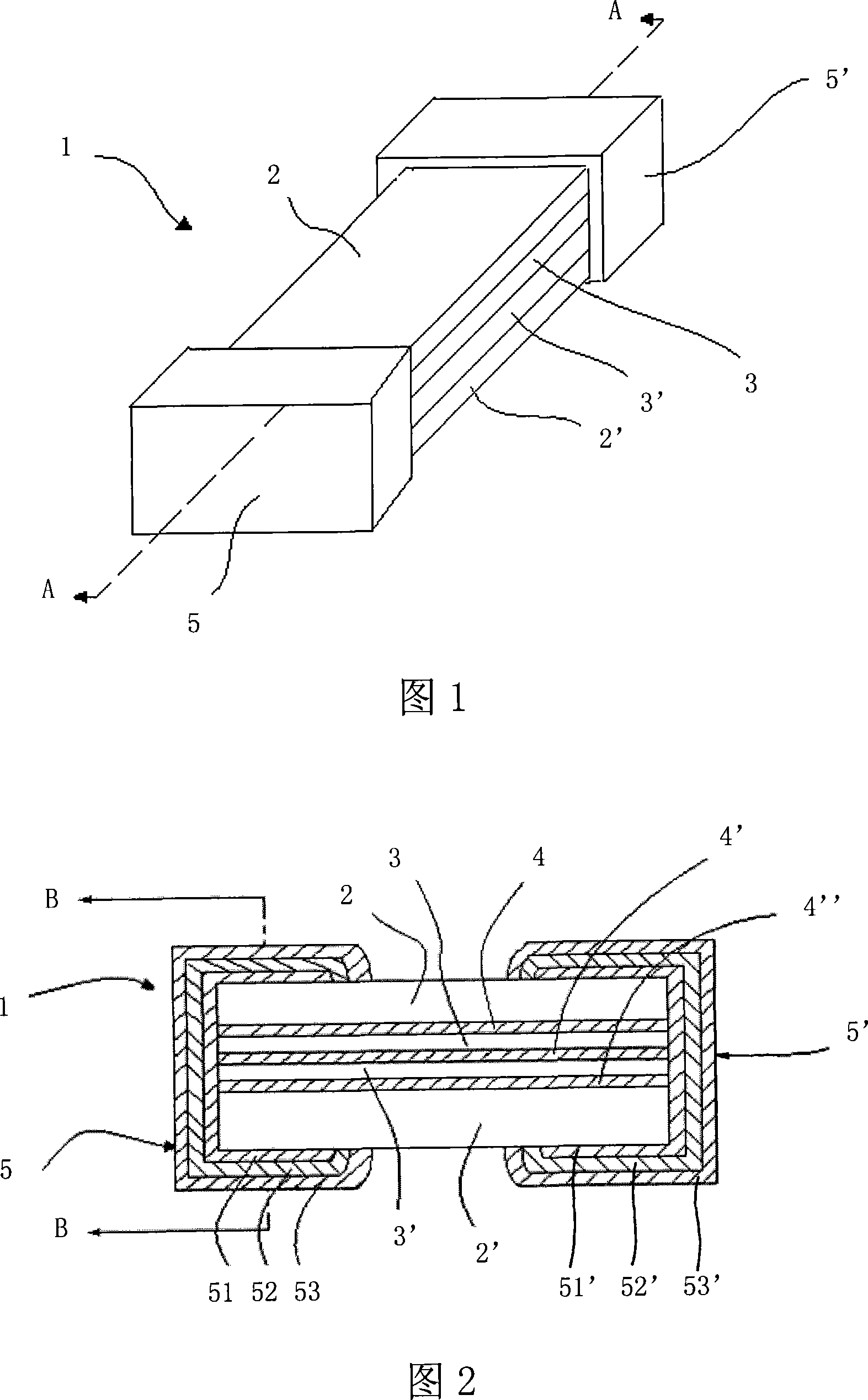
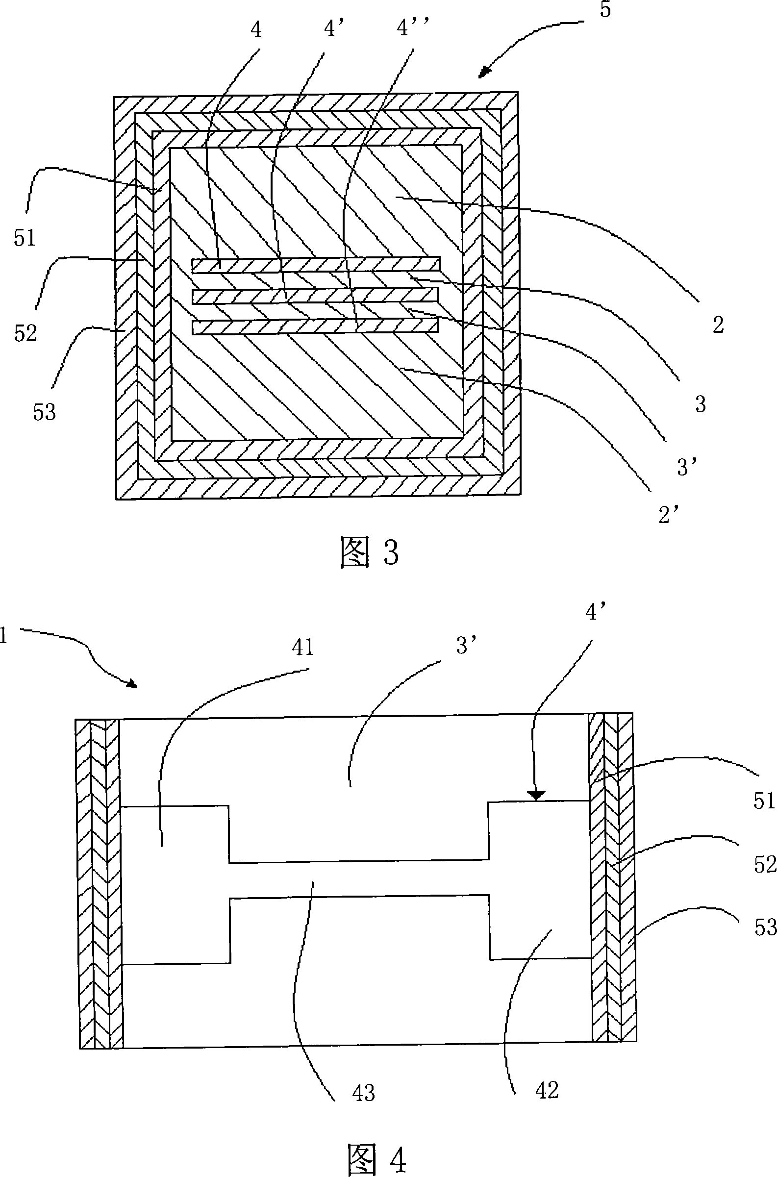
[0034] Please refer to Fig. 1 for a structural schematic diagram of the novel chip varistor of the present invention, Fig. 2 is a schematic diagram of a cross-sectional structure in the direction of A, Fig. 3 is a schematic diagram of a cross-sectional structure in the direction of B, and Fig. 4 is a top view of a ceramic-glass material layer with a piezoresistive film attached In the structural diagram, the proportions of each part are not strictly referred to in kind, but are enlarged for the convenience of explanation.

[0035] A new type of chip varistor 1 is composed of a glass-ceramic material layer, a varistor film and terminal electrodes covered at both ends, wherein the glass-ceramic material layer has four layers, which are used as the base layer, respectively It is the upper and lower surface base layers 2, 2' and the middle layer base layer 3, 3'. The inner surface of each base layer is attached with a piezoresistive film 4, 4', 4", and each layer is bonded together...


PUM


Abstract

This invention relates to a new type of slice voltage-sensitive resistors and a manufacturing method, in which, the resistor is composed of a glass-ceramic material layer, a voltage-sensitive resistor film and end-electrodes covering on both ends, the glass-ceramic material layer includes three or more layers adhered with a voltage-sensitive resistor film on each layer to comprise a monolithic structure, and the parallel arrayed voltage-sensitive resistor films in it are conducted to the end electrodes. The manufacturing method includes: preparing a glass-ceramic material layer as the base layer, adhering a layer of voltage-sensitive resistor film on the base layer, covering a layer of backings and repeating the above mentioned operations till getting the designed layers and raw membranes to be cut to voltage-sensitive resistors and sintered and sealing the end electrodes and plating it. Advantage: rated voltage and rated current are increased with consistency of resistance value and durability of solvent.

Description

technical field [0001] The invention relates to a line protection element, which is applied in the field of line protection, in particular to a novel chip varistor and a manufacturing method thereof. Background technique [0002] Surface mount varistors are widely used in the field of overcurrent protection, such as circuit boards that require high component miniaturization and integration. Compared to leaded varistors, surface mount types have smaller solder feet and take up less space. U.S. Patent No. 5658833 illustrates a method of manufacturing such a surface-mounted varistor. A varistor film is painted on an insulating layer, then covered with an insulating layer, and finally covered on the upper and lower insulating layers. A cover layer of another composition, so that a thin film varistor with good mechanical properties is obtained; the base material of some traditional surface mount varistors is a polymer material, which is used in US Patent No.5790587 The FR-4 epo...

Claims


Application Information

Patent Timeline
IPC IPC(8): H01C7/10H01C17/00
Inventor 苗明清周欣山沈十林
Owner SHANGHAI CHANGYUAN WAYON CIRCUIT PROTECTION CO LTD
Why Eureka
Try Eureka