Circuit capable of eliminating NMOS single tube transmission to form static short circuit current

A short-circuit current and circuit technology, applied in the direction of logic circuit coupling/interface, logic circuit connection/interface layout using field effect transistors, etc., can solve the problem of large circuit area consumption, exceeding noise tolerance, weakening the signal strength when transmitting high level and other problems, to achieve the effect of simple design steps, saving chip area, and avoiding static short-circuit current.

Active Publication Date: 2007-08-22
BEIJING MXTRONICS CORP +1
View PDF0 Cites 9 Cited by
  • Summary
  • Abstract
  • Description
  • Claims
  • Application Information

AI Technical Summary

Problems solved by technology

And, when the source voltage of the NMOS transistor rises, the voltage difference V between the source and the substrate sb It will cause the body effect and increase the threshold voltage, which will further weaken the strength of the signal when the high level is transmitted, and may exceed the noise tolerance of the next level
For the next-level CMOS circuit, when the high level is transmitted, the weakened input signal causes the PMOS tube to be unable to be effectively cut off, and the PMOS tube and the NMOS tube are in the simultaneous conduction state, which will generate a static short-circuit current. This current increases power consumption of the circuit
[0003] The existing common solution is to connect NMOS transistors and PMOS transistors in parallel to form dual-transistor transmission gates to eliminate the problem of threshold drop, but in some applications such as large-scale programmable logic devices, there are a large number of transmission gate circuits, such as multiple Selector switch, switch matrix, etc., if the dual-transistor transmission structure is used, the circuit area consumption will be too large
Another solution is to add a pressurized structure to compensate for the threshold drop by increasing the gate voltage of the NMOS transmission tube, but the disadvantage of this structure is that the circuit is too complicated and difficult to design
Another design is to add a feedback loop to the CMOS circuit, but due to the bidirectional conduction characteristics of the NMOS transmission tube, the function of the feedback loop can affect the input drive through the transmission tube, which may lead to circuit performance degradation or even functional failure.
Therefore, the existing design has the disadvantages of large circuit area consumption, complex structure, and great influence on the performance and function of the original circuit.

Method used


Image

  • Circuit capable of eliminating NMOS single tube transmission to form static short circuit current
  • Circuit capable of eliminating NMOS single tube transmission to form static short circuit current
  • Circuit capable of eliminating NMOS single tube transmission to form static short circuit current

Examples


Embodiment Construction

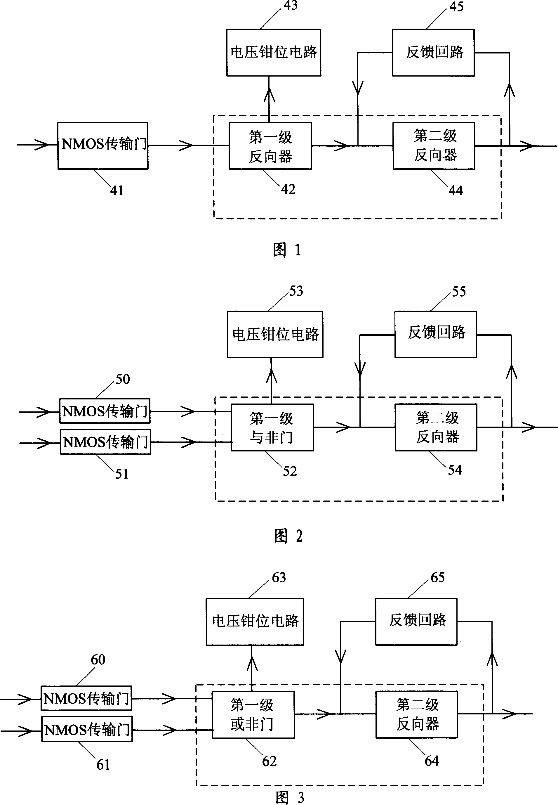
[0026] As shown in FIG. 1 and FIG. 4 , the NMOS transmission gate 41 is composed of the NMOS transmission transistor 11 , the voltage clamping circuit 43 is composed of the PMOS transistor 14 , and the feedback loop 45 is composed of the PMOS transistor 17 . When D1=1 (power supply voltage VDD), the NMOS transmission tube 11 is turned on through the control signal S1, and a high level VDD-V with a threshold drop is output th , the NMOS transistor 12 is turned on, and the source voltage of the PMOS transistor 13 is clamped at VDD-V by the PMOS transistor 14 th , so the source-gate voltage difference of the PMOS transistor 13 is less than the threshold voltage, the PMOS transistor 13 is guaranteed to be cut off, and the static short-circuit current generation is avoided at this stage; the first-stage inverter 42 outputs a low level, and the second-stage inverter In 44, the NMOS transistor 15 is turned off, the PMOS transistor 16 is turned on, the second-stage inverter 44 outputs...


PUM


Abstract

A circuit used for eliminating static shortcircuit current formed by transmission of NMOS single tube consists of NMOS transmission tube and CMOS buffer circuit with two CMOS reverse controller circuits. It is featured as coupling one voltage clamp circuit between power supply end and master current path of the first CMOS reverse controller and bridge-jointing a feedback loop with input end and output end of the second CMOS reverse controller.

Description

technical field [0001] The invention relates to a circuit structure. Background technique [0002] The NMOS transmission tube has good characteristics of low-level transmission, but poor performance of high-level transmission. When the NMOS tube transmits a high level, it cannot pull up the voltage of the source to exceed VDD-V th , this voltage loss is called threshold drop. And, when the source voltage of the NMOS transistor rises, the voltage difference V between the source and the substrate sb It will cause the body effect and increase the threshold voltage, which will further weaken the strength of the signal when the high level is transmitted, and may exceed the noise tolerance of the next stage. For the next-level CMOS circuit, when the high level is transmitted, the weakened input signal causes the PMOS tube to be unable to be effectively cut off, and the PMOS tube and the NMOS tube are in the simultaneous conduction state, which will generate a static short-circu...

Claims


Application Information

Patent Timeline
Patent Type & Authority Applications(China)
IPC IPC(8): H03K19/0185
Inventor 文治平李学武陈雷周涛张帆杜忠刘增容张彦龙储鹏
Owner BEIJING MXTRONICS CORP
Why Eureka
Try Eureka