Process for preparing Cu2ZnSnS4 semiconductor thin film solar cell

A solar cell and semiconductor technology, applied in semiconductor devices, sustainable manufacturing/processing, circuits, etc., can solve problems such as complex processes, and achieve the effects of easy formation, simple operation and use, and avoiding the loss of elements

Inactive Publication Date: 2007-08-29
UNIV OF SCI & TECH BEIJING
View PDF0 Cites 24 Cited by
  • Summary
  • Abstract
  • Description
  • Claims
  • Application Information

AI Technical Summary

Problems solved by technology

However, this method also does not break away from the two steps of the aforementioned preparation scheme,

Method used


Image

  • Process for preparing Cu2ZnSnS4 semiconductor thin film solar cell
  • Process for preparing Cu2ZnSnS4 semiconductor thin film solar cell

Examples


example 1

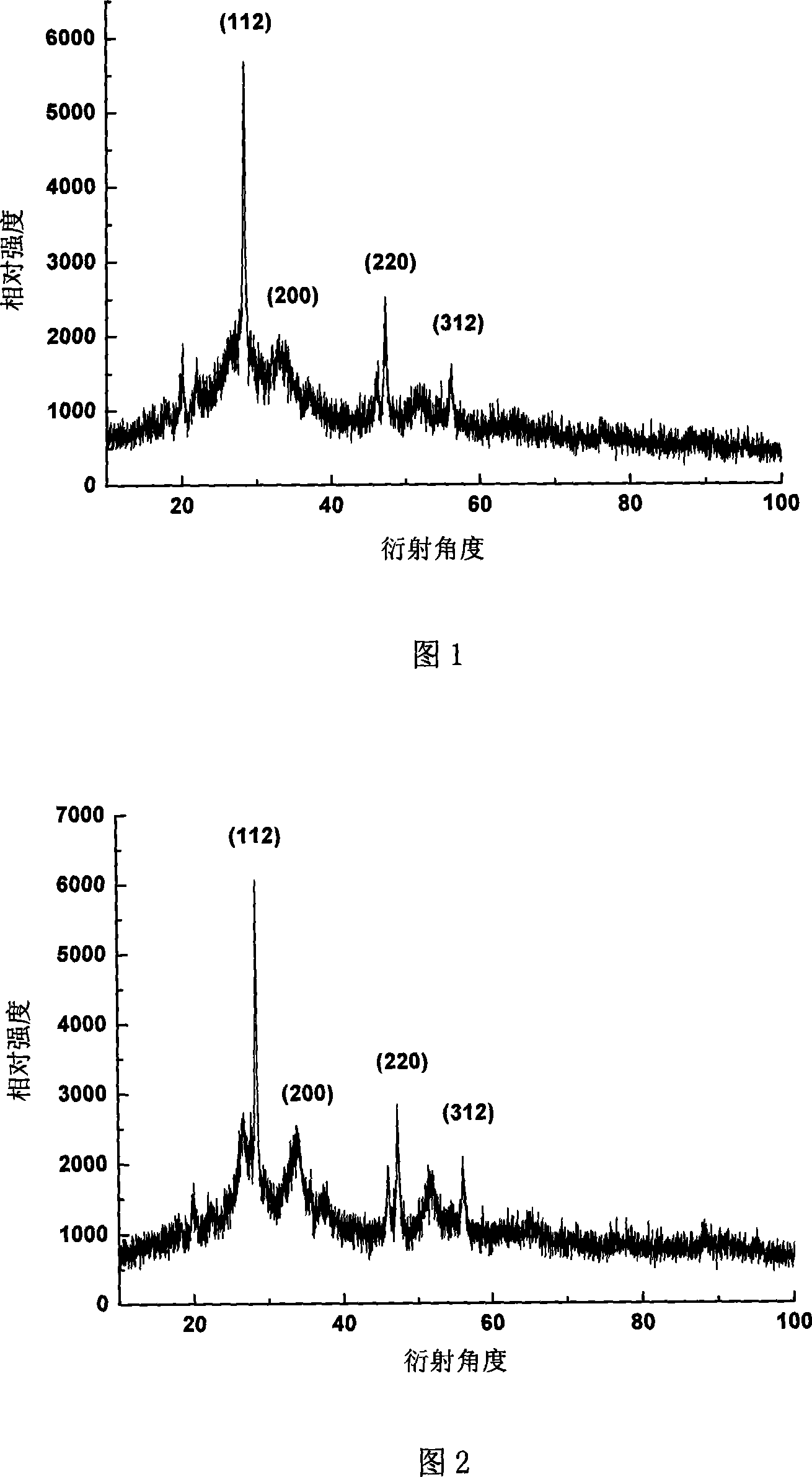
[0021] Example 1: Cu 2 ZnSnS 4 N of the absorbing layer 2 Atmosphere (350°C) preparation

[0022] (1) Place the molybdenum sheet (or conductive glass) coated with the slurry in a resistance furnace and pass N 2 Exclude air for fifteen minutes, then preheat at 50°C for ten minutes.

[0023] (2) Raise the temperature to 200°C at a rate of 10°C / min, and keep it warm for one hour.

[0024] (3) Heat up from 200°C to 350°C at a rate of 2°C / min, keep warm for two hours, then cool to room temperature with the furnace and take out to obtain a blue-black absorption layer.

example 2

[0025] Example 2: Cu 2 ZnSnS 4 N of the absorbing layer 2 Atmosphere (400°C) preparation

[0026] (1) Place the molybdenum sheet (or conductive glass) coated with the slurry in a resistance furnace and pass N 2 Exclude the air for fifteen minutes, then preheat at 50°C for ten minutes.

[0027] (2) Raise the temperature to 200°C at a rate of 10°C / min, and keep it warm for one hour.

[0028] (3) Heat up from 200°C to 400°C at a rate of 2°C / min, keep warm for two hours, then cool to room temperature with the furnace and take out to obtain a blue-black absorption layer.

example 3

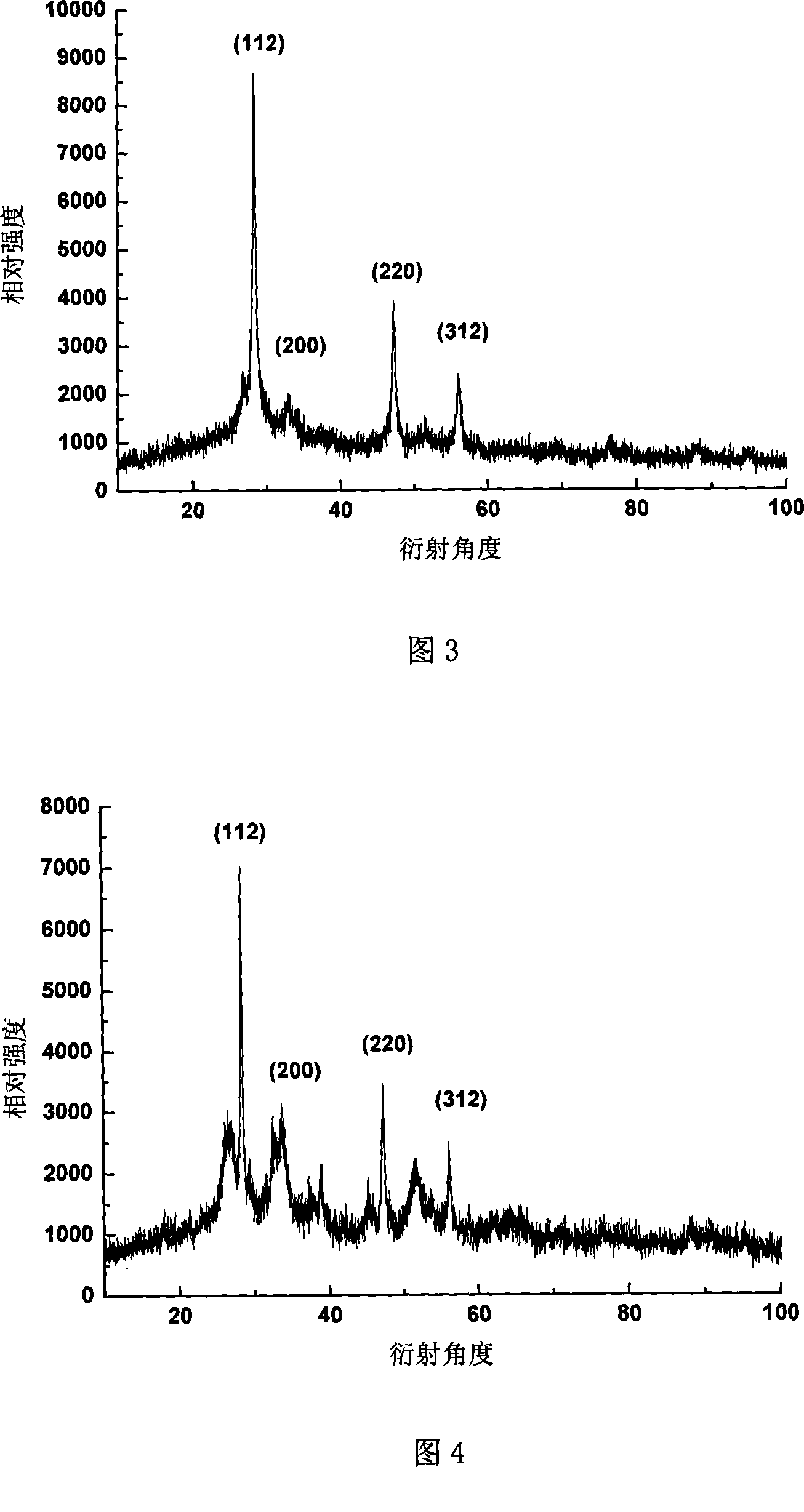
[0029] Example 3: Cu 2 ZnSnS 4 H of the absorbing layer 2 Atmosphere (350°C) preparation

[0030] (1) Place the molybdenum sheet (or conductive glass) coated with the slurry in a resistance furnace and pass through H 2 Exclude the air, check the purity three times, and then preheat at 50°C for ten minutes.

[0031] (2) Raise the temperature to 200°C at a rate of 10°C / min, and keep it warm for one hour.

[0032] (3) Heat up from 200°C to 350°C at a rate of 2°C / min, keep warm for two hours, then cool to room temperature with the furnace and take out to obtain a blue-black absorption layer.


PUM


Abstract

This invention relates to a technology for preparing Cu2ZnSnS4 semiconductor film solar cells, which mixes grains of Cu, Zn and Sn in the chemical measured ratio Cu : Zn : Sn=1.6-1.7 : 1 : 1 to press it to a cylindrical pressed shape in the diameter of 10mm and height of 15mm to be packaged in a quartz tube in the vacuum degree of 10-4-10-3pa to form an alloy ingot by inducing melt, then manufactures a brittle alloy thin strip of 15-30mum thick and 5-8mm wide by a strip-throwing technology, then mixes the strip with sulfur powder to be milled for 48-96 h to form black slurry to be coated on a Mo matrix or a glass matrix then to be dried and heated in H2 or N2 atmosphere, which can avoid loss of elements and guarantee strict chemical measurement ratio.

Description

technical field [0001] The invention belongs to the technical field of photovoltaic cells, and in particular provides a method for preparing Cu 2 ZnSnS 4 The process of semiconductor thin film solar cells. Background of the invention [0002] Cu 2 ZnSnS 4 It is a semiconductor material used as the absorber layer of thin film solar cells. It has a band gap of 1.5eV, 10 4 cm -1 The absorption coefficient is very in line with the conditions required by solar cells. The elements contained in the compound are all abundant in the earth's crust, and it does not contain the toxic metal Cd contained in other solar cell materials such as CdTe, nor does it contain CuInSe 2 The noble metal In used is a material that is very friendly to the environment and is suitable as an absorber layer of a solar cell, so it has a very broad application prospect. [0003] Research institutions in many countries have carried out research on this compound and made great progress. At present, th...

Claims


Application Information

Patent Timeline
IPC IPC(8): H01L31/18
CPCY02P70/50
Inventor 果世驹王璐鹏杨永刚聂红波王延来
Owner UNIV OF SCI & TECH BEIJING
Why Eureka
Try Eureka