Semiconductor device

A semiconductor and electrical connection device technology, applied in the direction of semiconductor devices, semiconductor/solid-state device components, electrical solid-state devices, etc., can solve problems such as passivation film damage, and achieve high withstand voltage performance, high light transmittance, and high reliability sexual effect

Inactive Publication Date: 2010-06-16
THE KANSAI ELECTRIC POWER CO +1
View PDF4 Cites 0 Cited by
  • Summary
  • Abstract
  • Description
  • Claims
  • Application Information

AI Technical Summary

Problems solved by technology

As a result, the SiC diode element 90 itself or the passivation film 98 of silicon dioxide or the like is destroyed

Method used


Image

  • Semiconductor device
  • Semiconductor device
  • Semiconductor device

Examples


Embodiment Construction

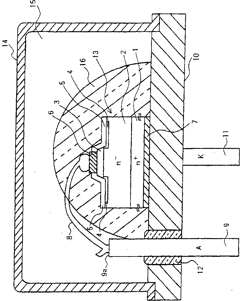
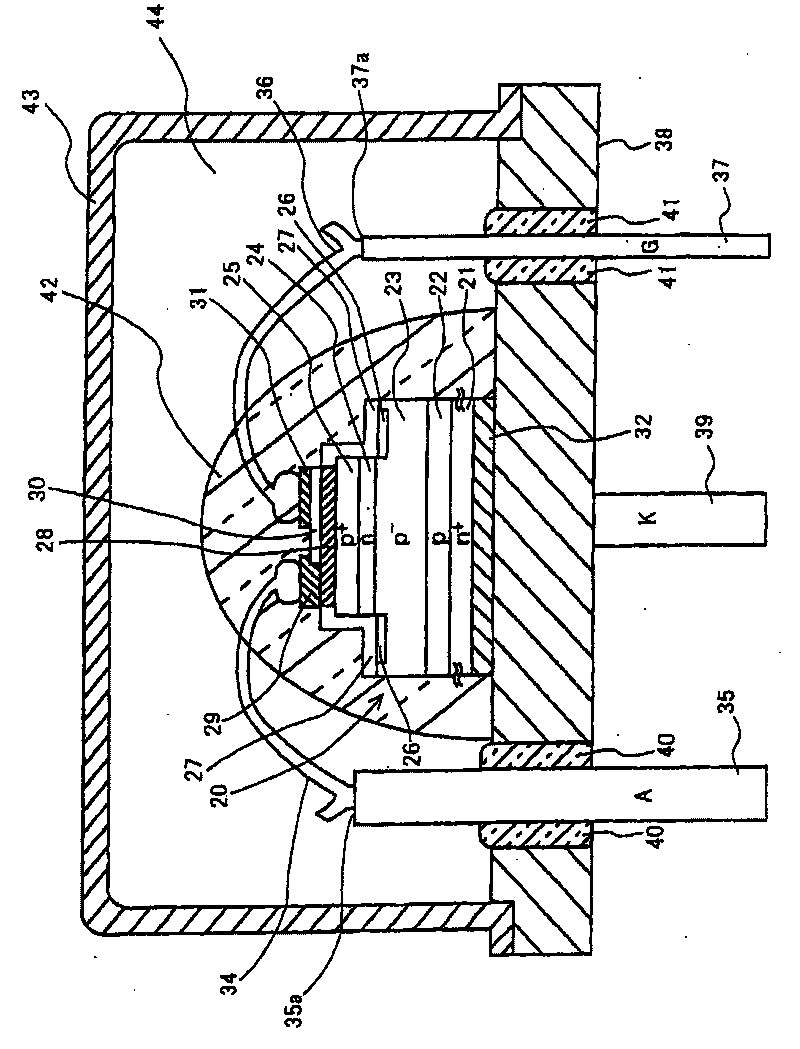
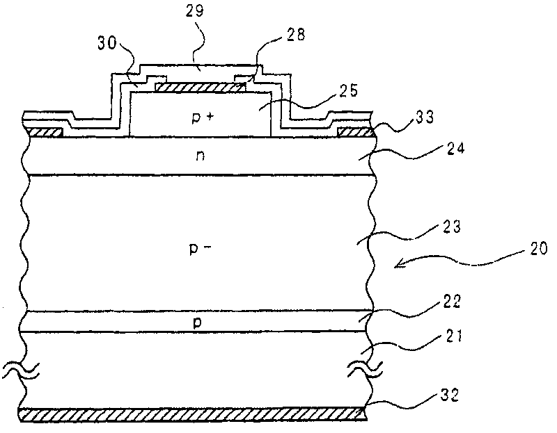
[0073] Preferred embodiments of the present invention will be described below. In an embodiment of the present invention, for a high heat-resistant and high-voltage-resistant semiconductor device, a synthetic polymer compound that cures a silicon-containing curable composition is used to coat the semiconductor device contained in the above-mentioned high-heat-resistant and high-voltage-resistant semiconductor device. A semiconductor element and at least a part of an electrical connection device for electrically connecting the semiconductor element to an external device.

[0074] The said silicon-containing curable composition of this invention contains at least 1 type of silicon-containing polymer among (A) component, (B) component, and (C) component demonstrated in detail below. When the silicon-containing curable composition does not contain (C)component, it contains both (A)component and (B)component. Furthermore, the silicon-containing curable composition further contains...


PUM

PropertyMeasurementUnit
particle diameteraaaaaaaaaa

Abstract

The external surface of a wide energy-gap semiconductor component is coated with a macromolecular compound synthesized from one or more siliceous polymers in cross-linked structure formed by Si-O-Si bonding. For example, the synthesized macromolecular compound is a siliceous polymer with one, two or more types of reaction base groups (A') selected from Si-R1, Si-O-R2, and Si-R3-OCOC(R4)=CH2, one or more parts in cross-linked structure formed by Si-O-Si bonding, and ingredients in average molecular weight <1000 less than 20 wt.%.

Description

technical field [0001] The present invention relates to a semiconductor device having high heat resistance and high voltage resistance. Background technique [0002] Silicon (hereinafter referred to as Si) semiconductor material is often used in semiconductor devices for converting electric signals and electric power, and various improvements are being made so that they can be used even in harsher temperature environments. Examples thereof include semiconductor devices mounted on artificial satellites and the like and used in space, and high-speed, highly integrated microprocessing devices mounted on computers. In addition, as other examples, various single semiconductor devices such as IGBTs mounted in various power integrated circuits that control electric power of hundreds of milliwatts or more, and in the engine compartment of automobiles, and the like. In addition, compound semiconductor materials can be used in various light-emitting semiconductor devices that emit li...

Claims


Application Information

Patent Timeline
Patent Type & Authority Patents(China)
IPC IPC(8): H01L23/29C08L83/07C08L83/05
CPCH01L2924/01046H01L23/3121H01L2924/0105H01L2224/4823H01L2924/01004H01L2924/16152H01L23/045H01L2924/01025H01L2924/13091H01L2924/01019H01L2924/01029H01L23/296H01L2225/06555H01L2224/48091H01L2924/01013H01L23/48C08G77/70H01L23/04H01L2224/8592H01L24/45H01L33/56H01L2224/48137H01L2924/01079H01L24/48H01L2224/48465H01L25/0657H01L2924/14H01L23/145C08G77/14H01L2225/0651H01L2924/0102C08L83/04H01L2924/01078H01L2924/01014H01L2224/45144H01L2924/01012H01L23/295C08G77/20H01L2225/06582H01L2924/12044H01L2924/13063C08G77/12H01L2924/13055H01L2924/1301H01L2924/1305H01L2924/13062H01L2224/45015H01L2924/12036H01L2924/12043H01L2924/00014H01L2924/00
Inventor 菅原良孝东海林义和
Owner THE KANSAI ELECTRIC POWER CO
Why Eureka
Try Eureka