Supercharge Your Innovation With Domain-Expert AI Agents!

LED vapor film pattern forming method and device

A light-emitting diode and evaporation technology, which is applied in the field of light-emitting diode evaporation film pattern formation, can solve the problems of cumbersome, complicated, and difficult to manufacture lithography etching process.

Inactive Publication Date: 2007-10-24
TYNTEK
View PDF0 Cites 0 Cited by
  • Summary
  • Abstract
  • Description
  • Claims
  • Application Information

AI Technical Summary

Problems solved by technology

[0004] However, the above-mentioned methods all need to use lithographic etching process to complete the fabrication of electrodes, but the lithographic etching process is quite cumbersome and complicated, and has high difficulty in fabrication.

Method used


Image

  • LED vapor film pattern forming method and device
  • LED vapor film pattern forming method and device
  • LED vapor film pattern forming method and device

Examples


Embodiment Construction

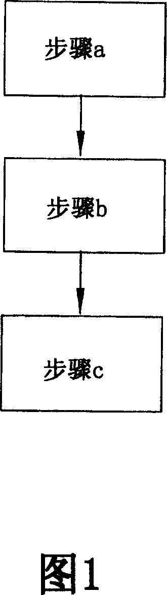
[0024] Please refer to Fig. 1, the method of the present invention comprises the following steps:

[0025] Step a: placing the carrier above the magnetic adsorption element;

[0026] Step b: placing the chip on the carrier; and

[0027] Step c: placing a non-magnetic metal mask on the surface of the chip, and using a magnetic adsorption element to absorb the non-magnetic metal mask to clamp and fix the chip to facilitate evaporation.

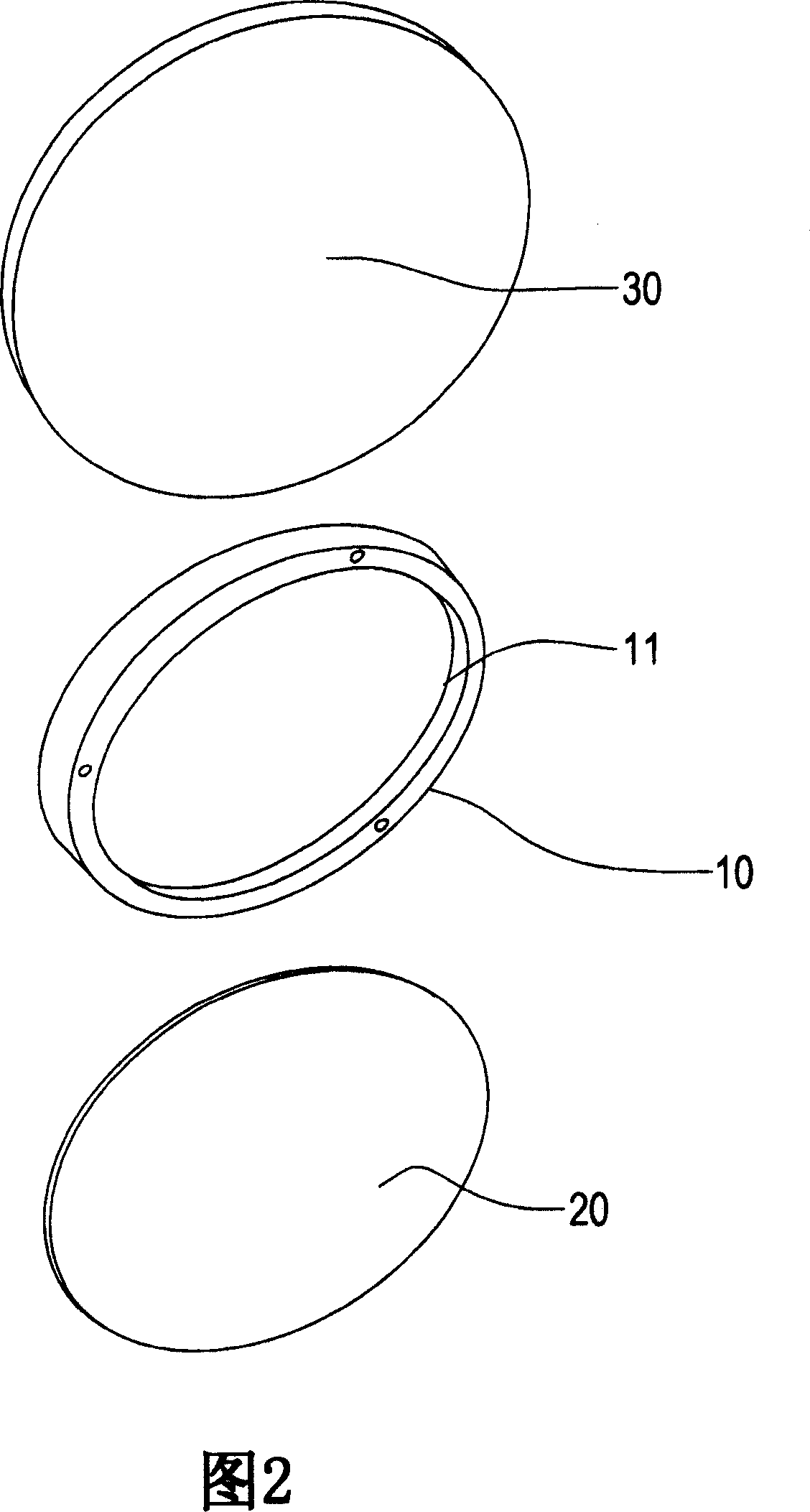
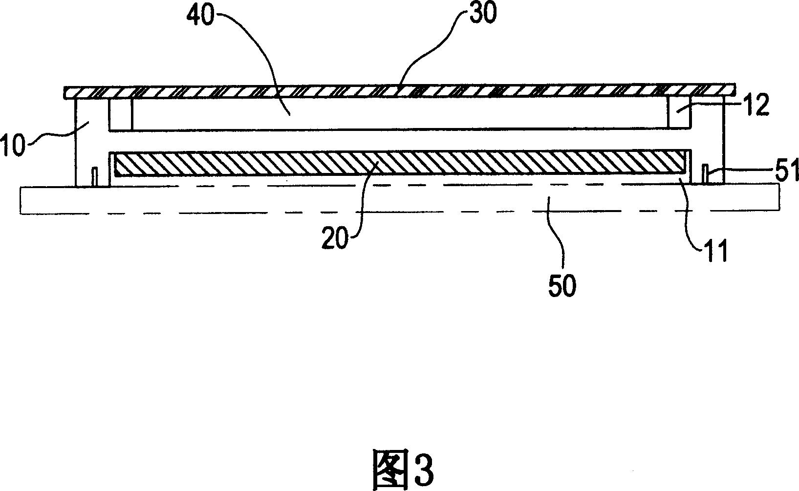
[0028] The device of the present invention comprises a carrier 10, a magnetic adsorption element 20 and a non-magnetic metal cover 30, as shown in FIG. A frame of appropriate length is extended above and below the peripheral edge of the carrier 10 so that accommodating spaces 11 and 12 are respectively formed above and below the carrier 10, and several positioning holes are provided on one side frame of the carrier 10.

[0029] The magnetic adsorption element 20 is provided in accordance with the shape of the carrier 10 and provided in the acc...


PUM


Abstract

The related forming method for film pattern of LED comprises: a. putting the carrier above the magnetic element; b. putting the chip in the carrier; and c. arranging a non-magnetic metal cover on chip surface, and adsorbing the cover to fix the chip for evaporation. This invention can reduce cost greatly.

Description

technical field [0001] The invention relates to a method and device for forming a light-emitting diode evaporated film pattern that greatly reduces manufacturing costs and enables products to be mass-produced. It is especially suitable for use in the manufacture of light-emitting diode electrodes or similar structures. Background technique [0002] Due to low power consumption and small size, light-emitting diodes are currently widely used in indicator lights of home appliances, backlights of mobile phones, traffic signs, advertising billboards, and third brake lights of automobiles. The general manufacturing method of light-emitting diodes is to make III-V compound chips first, then make metal electrodes on the III-V compound chips, then cut to form light-emitting diode crystal grains, and finally carry out packaging operations to complete the light-emitting diodes. make. [0003] The existing manufacturing methods of the metal electrodes of light-emitting diodes can be ro...

Claims


Application Information

Patent Timeline
Patent Type & Authority Applications(China)
IPC IPC(8): H01L33/00H01L21/285C23C14/04C23C14/24
Inventor 龚正
Owner TYNTEK
Features
  • R&D
  • Intellectual Property
  • Life Sciences
  • Materials
  • Tech Scout
  • Unparalleled Data Quality
  • Higher Quality Content
  • 60% Fewer Hallucinations
Learn More