High-curren density heterogeneous beam electron source
A technology of high current density and beam electrons, applied in the field of electric vacuum, can solve the problems of increasing the volume and weight of devices
- Summary
- Abstract
- Description
- Claims
- Application Information
AI Technical Summary
Problems solved by technology
Method used
Image
Examples
Embodiment 1
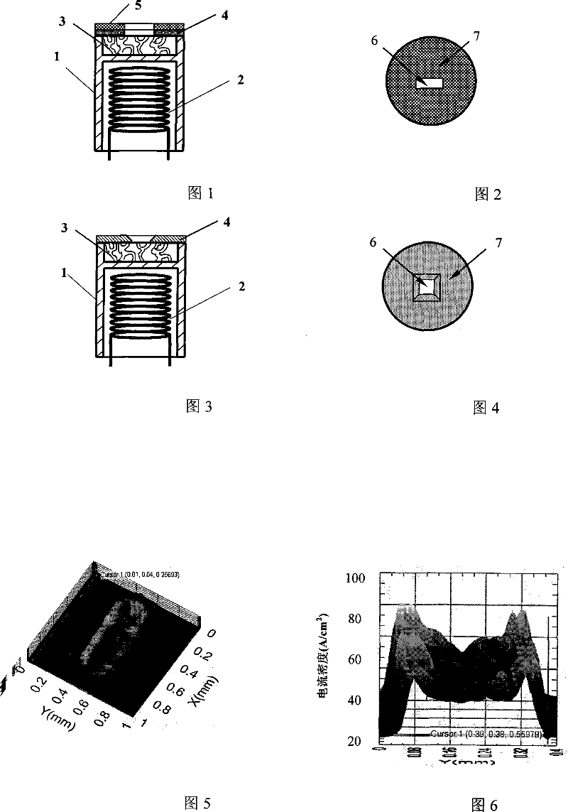
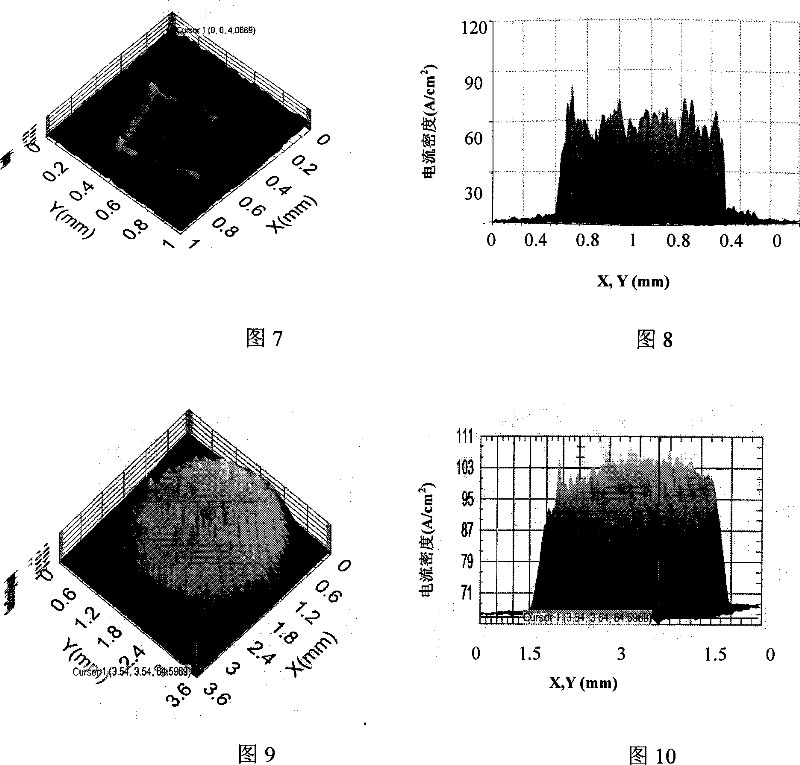
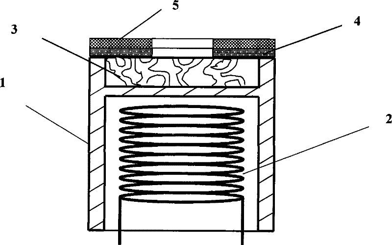
[0027] Embodiment 1 is used to provide the structure of the high current density special-shaped beam electron source, including the Mo sleeve, the heater matched with the molybdenum sleeve, the scandium oxide doped impregnated cathode assembled with the molybdenum sleeve, and the refractory metal tungsten Solid overlay. The cathode and the molybdenum sleeve are welded together by laser welding, and a heater is embedded under the sleeve to heat the cathode. EDM is used to process a rectangular area with an angle of 60 degrees between the side wall of the hole and the surface on the tungsten covering layer with a thickness of 50 microns. The lengths of the two sides are 200 microns and 800 microns respectively. , the average current density in the emission area reaches 55A / cm 2 , the maximum emission of the edge is 85A / cm 2 , and work stably for 120 hours under this condition. (see structure image 3 , rectangular beam shape and current distribution see Figure 5 and Figu...
Embodiment 2
[0028] Embodiment 2 is used to provide the structure of the high current density special-shaped beam electron source, including the Mo sleeve, the heater matched with the molybdenum sleeve, the scandium oxide doped pressed cathode assembled with the molybdenum sleeve, and the solid covering of noble metal niobium layer. The cathode and the molybdenum sleeve are welded together by laser welding, and a heater is embedded under the sleeve to heat the cathode. Laser micromachining technology is used to process a rectangular area with an angle of 80 degrees between the side wall of the hole and the surface on the niobium covering layer with a thickness of 100 microns. The lengths of the two sides are 100 microns and 400 microns respectively. When working, the average current density in the emission area reaches 50A / cm 2 , the maximum emission of the edge is 85A / cm 2 , and work stably for 200 hours under this condition.
Embodiment 3
[0029] Embodiment 3 is used to provide the structure of the high current density special-shaped beam electron source, including the Mo sleeve, the heater matched with the molybdenum sleeve, the scandium oxide doped impregnated cathode assembled with the molybdenum sleeve, and the entity of the tungsten-molybdenum alloy overlay. The cathode and the molybdenum sleeve are welded together by laser welding, and a heater is embedded under the sleeve to heat the cathode. EDM is used to process a rectangular area on the tungsten-molybdenum alloy covering layer with a thickness of 10 microns. The side wall of the hole is perpendicular to the surface. , the average current density in the emission area reaches 55A / cm 2 , the edge maximum emission is 90A / cm 2 , and work stably for 200 hours under this condition.
PUM
 Abstract
Description
Claims
Application Information


