Double-inlay structure and its making method

A dual damascene structure and manufacturing method technology, which is applied in semiconductor/solid-state device manufacturing, electrical components, electrical solid-state devices, etc., can solve problems such as inter-metal dielectric layer damage, inter-metal dielectric layer surface damage, and difficulty in cleaning, etc., to achieve increased Large parasitic capacitance, the effect of increasing device reliability and stability

Inactive Publication Date: 2007-11-28
SEMICON MFG INT (SHANGHAI) CORP
View PDF1 Cites 36 Cited by
  • Summary
  • Abstract
  • Description
  • Claims
  • Application Information

AI Technical Summary

Problems solved by technology

[0005] Therefore, the object of the present invention is to provide a dual damascene structure and its manufacturing method to solve the problem in the prior art that chemical mechanical grinding causes damage to the intermetallic dielectric layer with a smaller hardness and a lower dielectr

Method used


Image

  • Double-inlay structure and its making method
  • Double-inlay structure and its making method
  • Double-inlay structure and its making method

Examples


Embodiment Construction

[0070] In order to make the above objects, features and advantages of the present invention more comprehensible, specific implementations of the present invention will be described in detail below in conjunction with the accompanying drawings.

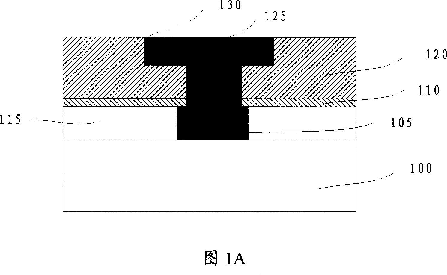
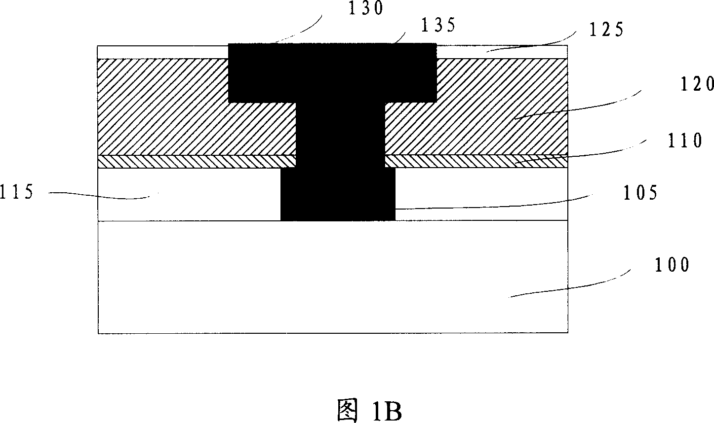
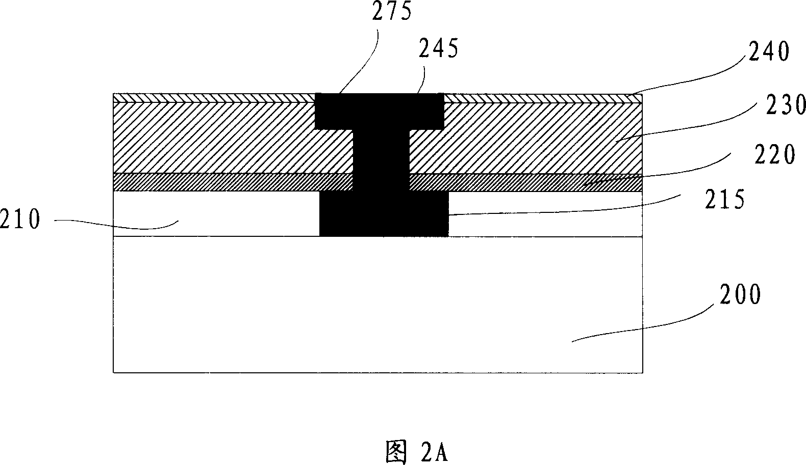
[0071] 2A and 2B are schematic cross-sectional views of the dual damascene structure of the present invention. FIG. 2A shows the first embodiment of the dual damascene structure of the present invention. A dielectric layer 210 is provided on a semiconductor substrate 200 . A metal pattern layer 215 is formed on the dielectric layer 210 through a photolithography process and an etch process, and the metal pattern layer 215 may be aluminum or copper. An etching stop layer 220 is formed on the metal pattern layer 215 and the dielectric layer 210 . The etch stop layer can be one or more layers. The function of the etching stop layer 220 is to prevent the metal of the metal pattern layer 215, such as copper, from diffusing upward; damag...


PUM

PropertyMeasurementUnit
Thicknessaaaaaaaaaa
Thicknessaaaaaaaaaa

Abstract

The invention discloses a making method of double-mosaic structure, which comprises the following steps: making burying covering layer on the metal dielectric layer to form the metal dielectric layer and through-hole and groove in the burying covering layer; covering etching stopping layer on the substrate with metal pattern; covering the metal dielectric layer on the etching stopping layer; forming burying covering layer on the metal dielectric layer; etching the groove and through-hole to sediment metal through photoetching; making the meta dielectric layer surface protected by burying covering layer from damaging in the moving photoetching agent course of chemical mechanic grinding and plasma; improving the reliability of elements.

Description

technical field [0001] The invention relates to the technical field of semiconductor manufacturing, in particular to a dual damascene structure and a manufacturing method thereof. Background technique [0002] The dual damascene process was developed in the context of increasingly smaller semiconductor devices using metallic copper for back-end interconnection. Different from the aluminum process, the copper process is to etch the through holes and trenches on the dielectric layer, and then use the deposition method to fill the metal copper into the through holes and trenches. Chinese Patent Application No. 02106882.8 discloses a dual damascene process, in which there are two types of processes: forming a through hole first and then forming a trench, and forming a trench first and then forming a through hole. The dual damascene process is shown in FIG. 1A , there is a dielectric layer 115 on the substrate 100 and a metal pattern layer 105 formed in the dielectric layer 115 ...

Claims


Application Information

Patent Timeline
IPC IPC(8): H01L23/522H01L21/768
Inventor 陈玉文
Owner SEMICON MFG INT (SHANGHAI) CORP
Why Eureka
Try Eureka