Semiconductor device, manufacturing method thereof, electro-optical device and electric device

A manufacturing method and semiconductor technology, applied in the fields of semiconductor/solid-state device manufacturing, semiconductor devices, semiconductor/solid-state device components, etc., can solve problems such as being unsuitable for mass production, requiring labor and time, etc.

Inactive Publication Date: 2007-12-12
SEIKO EPSON CORP
View PDF1 Cites 1 Cited by
  • Summary
  • Abstract
  • Description
  • Claims
  • Application Information

AI Technical Summary

Problems solved by technology

As a means of avoiding damage, although it is also possible to open a contact hole in the gate insulating layer by using a physical method such as a needle, it requires labor and time, and is not suitable for mass production.

Method used


Image

  • Semiconductor device, manufacturing method thereof, electro-optical device and electric device
  • Semiconductor device, manufacturing method thereof, electro-optical device and electric device
  • Semiconductor device, manufacturing method thereof, electro-optical device and electric device

Examples


no. 1 Embodiment

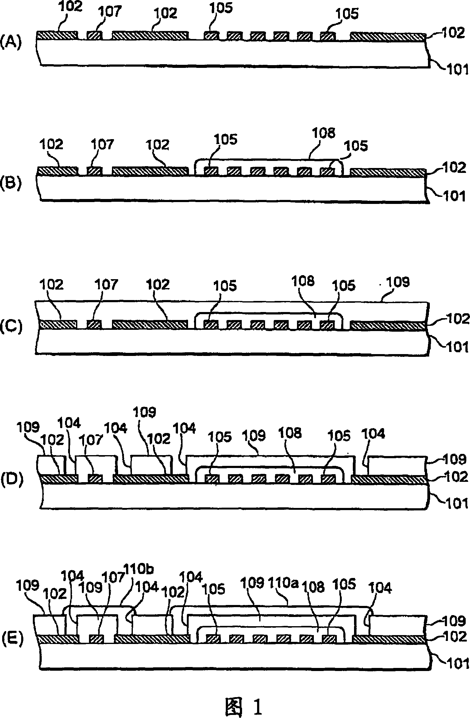
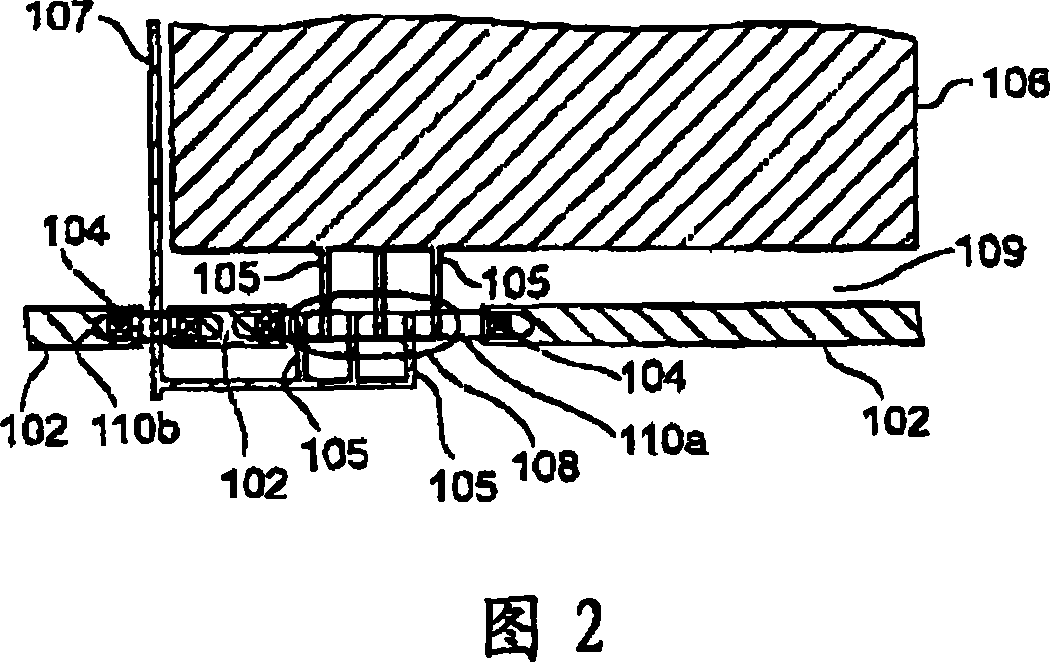
[0039] 1 to 4 show examples in which the organic semiconductor transistor of the present invention is used in a display pixel driving circuit. FIG. 1 is a process diagram illustrating a manufacturing process of an organic semiconductor transistor as a semiconductor device, and FIG. 2 is a plan view of a pixel driving circuit.

[0040] In this embodiment, low-resistance gate lines (wiring) have been formed on the substrate, and the connection between the gate lines and the formation of the gate electrodes are performed in the same process by the printing method.

[0041] First, as shown in FIG. 1(A), a first gate line 102, a data line 107, source and drain electrodes 105, a pixel electrode 106 (see FIG. 2), and an external drive device are formed together on an insulating substrate 101. Terminals for connection, external connection wiring, etc. (not shown).

[0042]As the insulating substrate 101 , for example, a plastic substrate such as PET (polyethylene terephthalate), or a...

no. 2 Embodiment

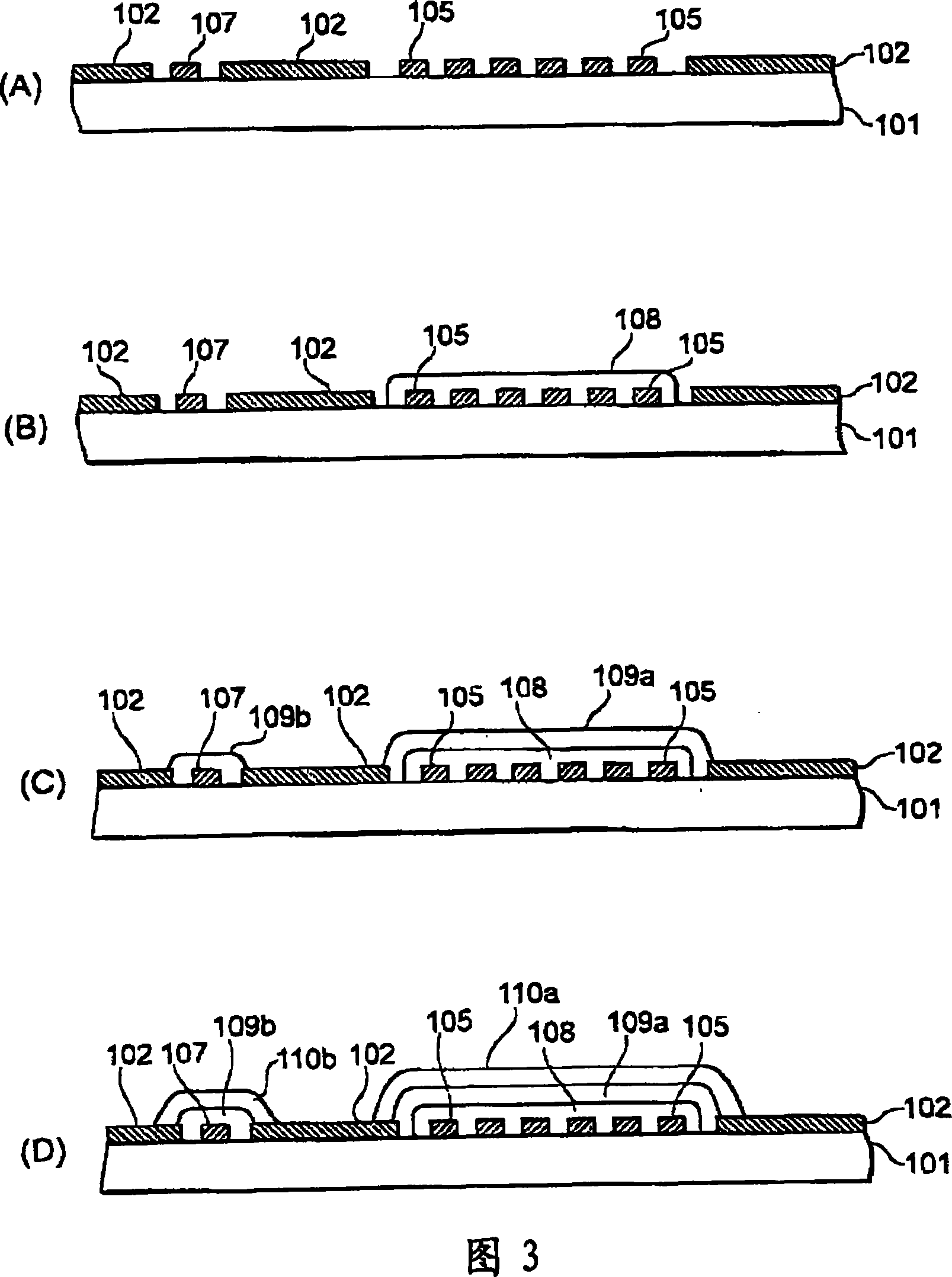
[0062] 3 and 4 show a second embodiment. 3 is a process diagram illustrating a manufacturing process of an organic semiconductor transistor as a semiconductor device, and FIG. 4 is a plan view of a pixel driving circuit. In FIG. 3 and FIG. 4 , the parts corresponding to those in FIG. 1 and FIG. 2 are denoted by the same reference numerals, and descriptions of these parts are omitted.

[0063] First, as shown in FIG. 3(A), a first gate line 102, a data line 107, source and drain electrodes 105, and a pixel electrode 106 (see FIG. 4 ) are formed together on an insulating substrate 101 to communicate with an external driving device. Terminals for connection, external connection wiring, etc. (not shown).

[0064] As shown in Figure (B), the substrate is treated with oxygen plasma and cleaned. Thereafter, F8T2 as an organic semiconductor is dropped and annealed by the inkjet method, and the organic semiconductor layer 108 is formed to have a film thickness of about 50 nm so as to...

no. 3 Embodiment

[0071] 5 and 6 show a third embodiment. 5 is a process diagram illustrating a manufacturing process of an organic semiconductor transistor as a semiconductor device, and FIG. 6 is a plan view of a pixel driving circuit. In FIG. 5 and FIG. 6 , the parts corresponding to those in FIG. 1 and FIG. 2 are given the same reference numerals, and descriptions of these parts are omitted.

[0072] In the third embodiment, the second gate line 110b, the first gate line 102 and the gate electrode 110a shown in the first embodiment (FIG. 1(E)) are composed of one gate electrode as shown in FIG. 5(E). wiring 110c. By constituting as described above, the number of patterns can be reduced, and the number of times of application by the inkjet method can be reduced, which is convenient.


PUM


Abstract

The present invention provides a semiconductor device which can reduce resistance value of used grid line (grid signal line), an electro-optical device and a electric device. The grid line transmits grid driven signal with organic semiconductor device in active matrix display. The semiconductor device includes an organic semiconductor transistor provided on a substrate; a data line connected to a source electrode or a drain electrode of the organic semiconductor transistor; and a gate line that is disposed so as to intersect the data line and that is connected to a gate electrode of the organic semiconductor transistor. In the semiconductor device, the gate line includes the gate electrode, a first gate line that transmits signals to the gate electrode, and a second gate line intersecting the data line, with an interlayer insulation layer therebetween; the gate electrode, the first gate line, and the second gate line are connected in series; and the electric conductivity of the first gate line is higher than the electric conductivity of the gate electrode and the electric conductivity of the second gate line.

Description

technical field [0001] The present invention relates to a semiconductor device, improvement of a manufacturing method of the semiconductor device, an electro-optical device and an electronic device using the semiconductor device. Background technique [0002] The technology of using organic semiconductor materials to fabricate semiconductor devices such as organic semiconductor transistors has been proposed. For example, in Publication No. 2005-215616, an example is described in which pixels, data lines, and peripheral lines are produced in one photolithography process, and then processed by a liquid phase process using a liquid material. Various functional films are formed to produce active matrix substrates. For example, in the film formation process using a liquid material, a conductive organic substance such as PEDOT (polyethylenedioxythiophene) is applied to a substrate by a printing method such as an inkjet method, and dried to form a circuit wiring. [0003] Patent ...

Claims


Application Information

Patent Timeline
Patent Type & Authority Applications(China)
IPC IPC(8): H01L27/28H01L23/522H01L21/84H01L21/768
CPCH01L27/3274H01L51/055H01L27/3279H10K59/125H10K59/1315H10K10/481
Inventor 守谷壮一川濑健夫
Owner SEIKO EPSON CORP
Why Eureka
Try Eureka