Organic light emitting device
A technology of organic light-emitting device and light-emitting layer, applied in the field of OLED, can solve problems such as difficulty in hole injection
- Summary
- Abstract
- Description
- Claims
- Application Information
AI Technical Summary
Problems solved by technology
Method used
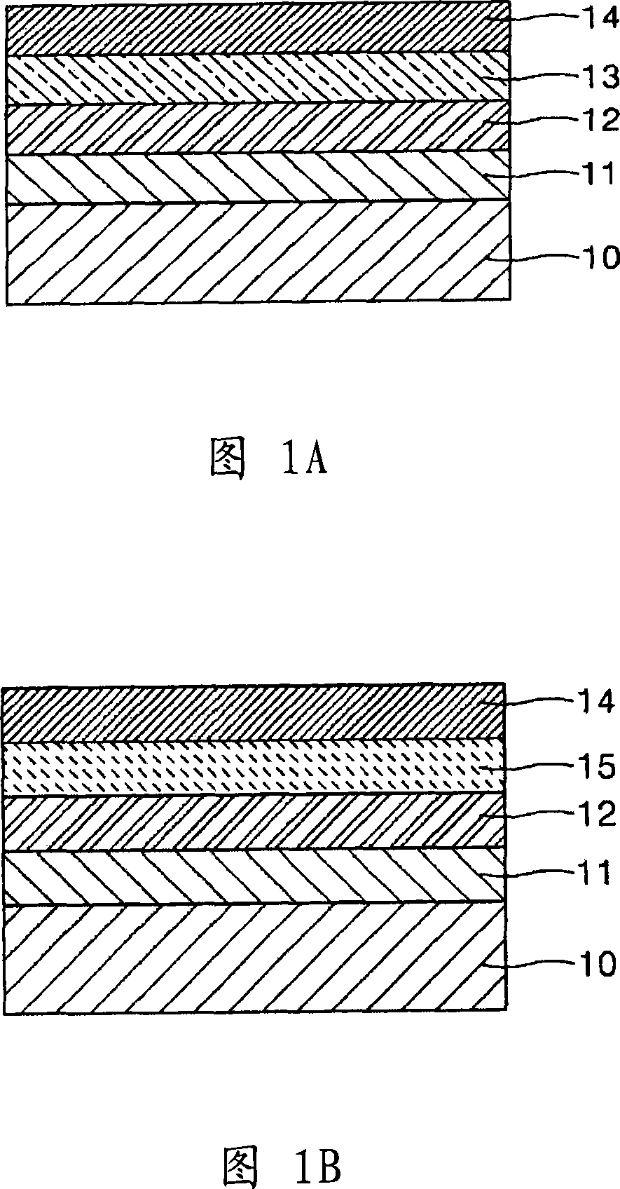
Image

Examples
preparation Embodiment 1
[0208] Preparation Example 1: Polyaniline (PANI) Conductive Polymer Composition
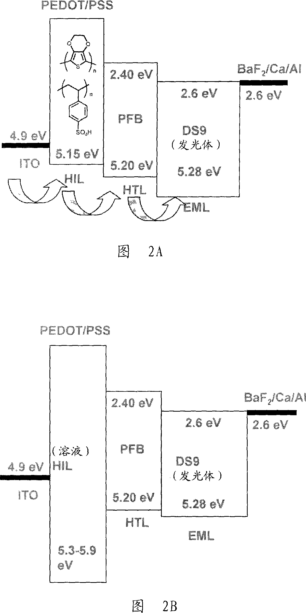
[0209] Polystyrenesulfonic acid-graft-polyaniline (PSSA-g-PANI) was polymerized as a self-doping conductive material using the known synthetic method of [W.J.Bae et al., Chem. Comm., pp2768-2769, 2003]. In this embodiment, the weight ratio of PSSA polymer chains and grafted PANI chains is 1:0.15. The number average molecular weight of PSSA-g-PANI was 35,000. This material was melted in water to 1.0% by weight. Then, a perfluorinated ionomer (PFI) was purchased from Aldrich Co., dispersed to 5 wt% in a solvent with a water to alcohol volume ratio of 0.45:0.55, and isopropanol and 5 wt% PFI at 1.0 wt% The PSSA-g-PANI solution was mixed and used as the material to form HIL 11. This sample is referred to as Sample A.
[0210] [Formula 14]
[0211]
[0212] (where x=1300, y=200, x=1)
preparation Embodiment 2
[0213] Preparation Example 2: Preparation of PEDOT-PSS / PFI Conductive Polymer Composition
[0214] PEDOT-PSS (model: Baytron P VP A14083) from H.C. Starck, a subsidiary of Bayer Aktien AG, was purified to control the Na and sulfate content to 5 ppm or less. Then, PFI of formula 14 was purchased from Aldrich Co. dispersed to 5 wt% in water and alcohol. Then, HIL 11 with each different composition of PEDOT-PSS was prepared. The proportions of this composition are listed in Table 1 below.
[0215] [Table 1]
[0216] sample code
Embodiment 1
[0217] Evaluation Example 1 - Work Function Evaluation of Conductive Polymer Films
[0218] The conductive polymer compositions obtained in Preparation Examples 1 and 2 were spin-coated on an ITO substrate to form a thin layer to a thickness of 50 nm, and heated on a hot plate in air at 200° C. for 5 minutes, and the conductive polymer was evaluated The work function of the composition. Surface Analyzer Model AC2 as a photoelectron spectrometer in air (PESA) manufactured by RIKEN KEIKI, Co., Ltd. was used as an evaluation apparatus. Sample A shows a work function of 5.6 eV, sample B shows a work function of 5.55 eV, sample C shows a work function of 5.63 eV, sample D shows a work function of 5.72 eV, and sample E shows a work function of 5.79 eV, and sample F showed a work function of 5.95 eV.
PUM
| Property | Measurement | Unit |
|---|---|---|
| thickness | aaaaa | aaaaa |
| thickness | aaaaa | aaaaa |
| thickness | aaaaa | aaaaa |
Abstract
Description
Claims
Application Information
 - R&D
- Intellectual Property
- Life Sciences
- Materials
- Tech Scout
- Unparalleled Data Quality
- Higher Quality Content
- 60% Fewer Hallucinations
Browse by: Latest US Patents, China's latest patents, Technical Efficacy Thesaurus, Application Domain, Technology Topic, Popular Technical Reports.
© 2025 PatSnap. All rights reserved.Legal|Privacy policy|Modern Slavery Act Transparency Statement|Sitemap|About US| Contact US: help@patsnap.com