

Solder lug and manufacturing method thereof
A technology of solder bumps and manufacturing methods, which is applied in the manufacture of semiconductor/solid-state devices, electrical components, and electrical solid-state devices, etc. problem, to achieve the effect of good physical connection, easy miniaturization and portability, and volume reduction
- Summary
- Abstract
- Description
- Claims
- Application Information
AI Technical Summary
Problems solved by technology
Method used
Image

Examples
Embodiment Construction
[0051] In order to make the purpose, features and advantages of the present invention more obvious and comprehensible, the specific implementation manners of the present invention will be described in detail below in conjunction with the accompanying drawings.
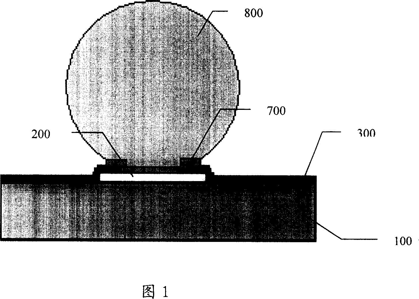
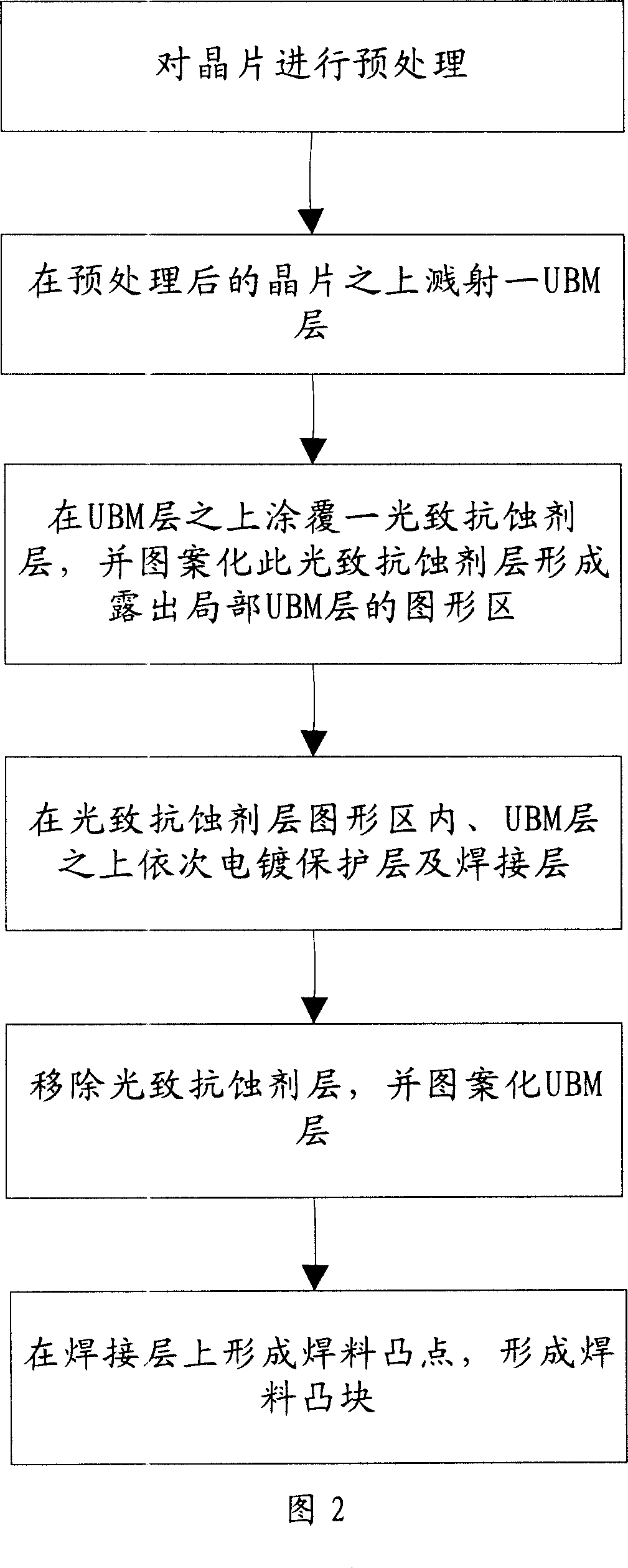
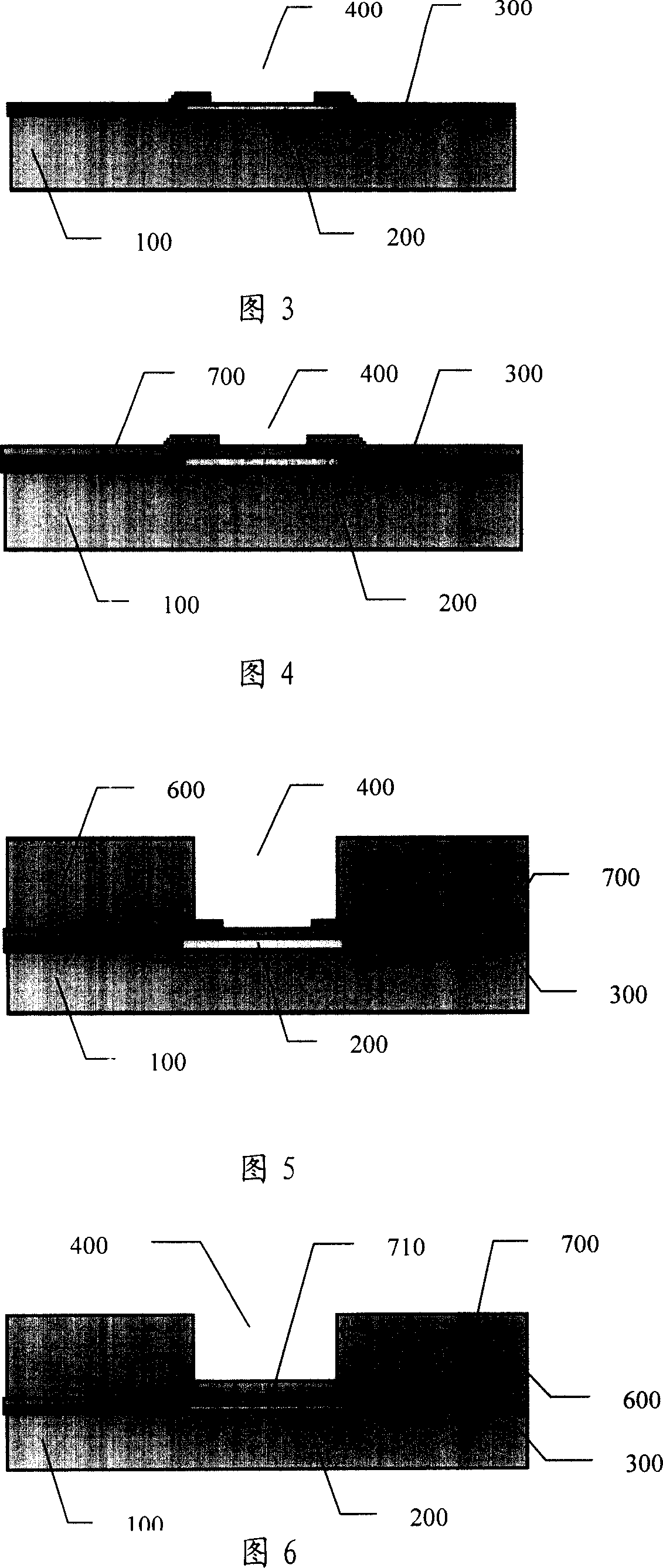
[0052] Fig. 2 shows the flow chart of manufacturing solder bumps of the present invention; As shown in Fig. 2, the manufacturing process of solder bumps comprises: the wafer 100 that comprises welding pad is carried out pretreatment; Sputtering on the wafer 100 after pretreatment A UBM layer 700 is shot; a photoresist layer 600 is coated on the UBM layer 700, and the photoresist layer 600 is patterned to form a pattern area that exposes the local UBM layer 700; In the pattern area of the resist layer 600, on the UBM layer 700, the protective layer 720 and the solder layer 720 are sequentially plated; the photoresist layer 600 is removed, and the UBM layer 700 is patterned; and then solder bumps 800 are formed on the s...
PUM
| Property | Measurement | Unit |
|---|---|---|
| Thickness | aaaaa | aaaaa |
| Thickness | aaaaa | aaaaa |
| Thickness | aaaaa | aaaaa |
Abstract
Description
Claims
Application Information