Pb-free sn-based material, wiring conductor, terminal connecting assembly, and pb-free solder alloy

A terminal connection and conductor technology, applied in the direction of metal/alloy conductor, metal material coating process, welding/cutting medium/material, etc., can solve problems such as short circuit of adjacent wiring materials, and achieve short circuit and high connection reliability Effect

Inactive Publication Date: 2008-01-02
HITACHI CABLE
View PDF5 Cites 49 Cited by
  • Summary
  • Abstract
  • Description
  • Claims
  • Application Information

AI Technical Summary

Problems solved by technology

However, with the lead-free Sn plating, especially in pure Sn plating, whiskers of needle-like crystals of Sn will be generated on the surface of the Sn plating film. As shown in Figure 2, these whiskers 5 may cause adjoining Short circuit between wiring materials (conductor 4)

Method used


Image

  • Pb-free sn-based material, wiring conductor, terminal connecting assembly, and pb-free solder alloy

Examples


Embodiment approach

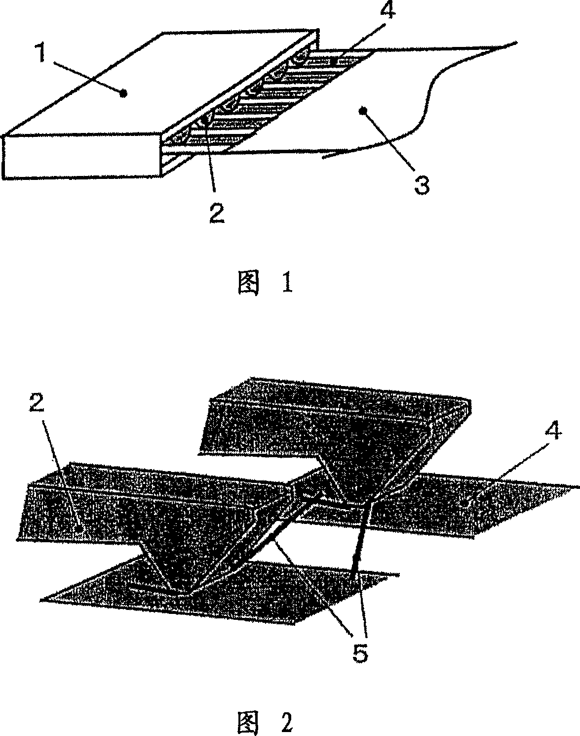
[0054] In the wiring conductor of the present embodiment, a Pb-free Sn plating film is provided on the entire surface (at least part of the surface) of a metal conductor, and a phase change retardation element layer and an oxidation suppressing element are provided on the upper layer of the Sn plating film The layer is then formed by reflow treatment, and has a Pb-free Sn coating layer on the entire surface of the metal conductor.

[0055] The Pb-free Sn coating layer is a layer mainly composed of an alloy of phase change delay elements, oxidation inhibitor elements, and Sn. The entire layer may be composed of alloys, or a part of the layer may have some phase change delay elements remaining Any one of a layer, a layer of an oxidation inhibiting element, and a Sn plating film.

[0056] Relative to the weight of the Sn plating film, the weight ratio of the layer of the phase change retardation element and the layer of the oxidation inhibitor is 0.001 to 10 wt%, preferably about 0.1...

Embodiment

[0067] Respectively adopt

[0068] (a) In pure Sn, 0.01wt% of phase change delay element (any one of Sb, Bi, In, Ag, Au, Ni, Ti, Zr, Hf) and 0.01wt% of oxidation inhibitor ( Any one of Ge, Zn, P, K, Mn, V, Si, Al, Mg, Ca) materials;

[0069] (b) Add 0.01wt% of phase change delay element (Bi), 0.01wt% of phase change delay element (Ni) and 0.01wt% of oxidation inhibitor (either P or Zn) to pure Sn. material;

[0070] (c) Add 1wt% of phase change delay element (any one of Sb, Bi, In, Ag, Au) and 0.01wt% of oxidation inhibitor (Zn, P, K, Mn, V) to pure Sn. Any one of) materials;

[0071] (d) Add 0.1wt% of phase change delay element (any one of Ni, Ti, Zr, Hf) and 0.01wt% of oxidation inhibitor (Si, P, Zn, Ge, Al, Any one of Mg and Ca) materials;

[0072] (e) In pure Sn, 1wt% of phase change delay element (Bi), 0.1wt% of phase change delay element (Ni), and 0.01wt% of oxidation inhibitor (either P or Zn) are added to the material ;

[0073] (f) A material in which only 0.01 wt% of pha...


PUM

PropertyMeasurementUnit
densityaaaaaaaaaa
densityaaaaaaaaaa
densityaaaaaaaaaa

Abstract

A Pb-free Sn-based material part of a wiring conductor is provided at least at a part of a surface the wiring conductor, and the Sn-based material part includes a base metal doped with a transformation retardant element and an oxidation control element. The transformation retardant element is at least one element selected from a group consisted of Sb, Bi, Cd, In, Ag, Au, Ni, Ti, Zr, and Hf. The oxidation control element is at least one element selected from a group consisted of Ge, P, Zn, Kr, Cr, Mn, Na, V, Si, Al, Li, Mg and Ca. The wiring conductor is reflow processed, such that at least one of the Sn, the transformation retardant element and the oxidation control element is diffused to form an alloy.

Description

Technical field [0001] The present invention relates to Pb-free Sn-based materials, wiring conductors, terminal connection parts, and Pb-free soldering alloys used in electronic equipment. Background technique [0002] Conventionally, in order to prevent oxidation on the surface of wiring materials, especially wiring materials made of copper and copper alloys, Sn plating, Ag plating, Au plating, or Ni plating are applied. For example, as shown in Figure 1, in the terminal connection part of the connector 1 and the flexible flat cable (hereinafter referred to as "FFC") 3, the connection pin (metal terminal) 2 and the conductor of the FFC3 of the connector (connection member) 1 The surface of 4 is plated. Among them, Sn is low in cost and excellent in industry, so wiring materials with Sn plated on the surface are generally widely used. As the alloy for Sn plating, a Sn-Pb alloy with good whisker resistance has been used conventionally. [0003] However, in recent years, due to env...

Claims


Application Information

Patent Timeline
Patent Type & Authority Applications(China)
IPC IPC(8): C22C13/00H01B1/02B23K35/24
CPCC22C13/00C22C13/02C23C28/023C23C28/021H05K2201/0769H05K3/244C23C26/02C23C26/00Y10T29/53209
Inventor 西甫辻隆之山野边宽冲川宽
Owner HITACHI CABLE
Why Eureka
Try Eureka