Input interface circuit adapted to both of analog and digital signals
A technology for inputting interface circuits and circuits, which can be used in digital transmission systems, negative feedback circuit layout, logic circuit connection/interface layout, etc., and can solve the problems of reducing chip size and cost.
- Summary
- Abstract
- Description
- Claims
- Application Information
AI Technical Summary
Problems solved by technology
Method used
Image

Examples
no. 1 example
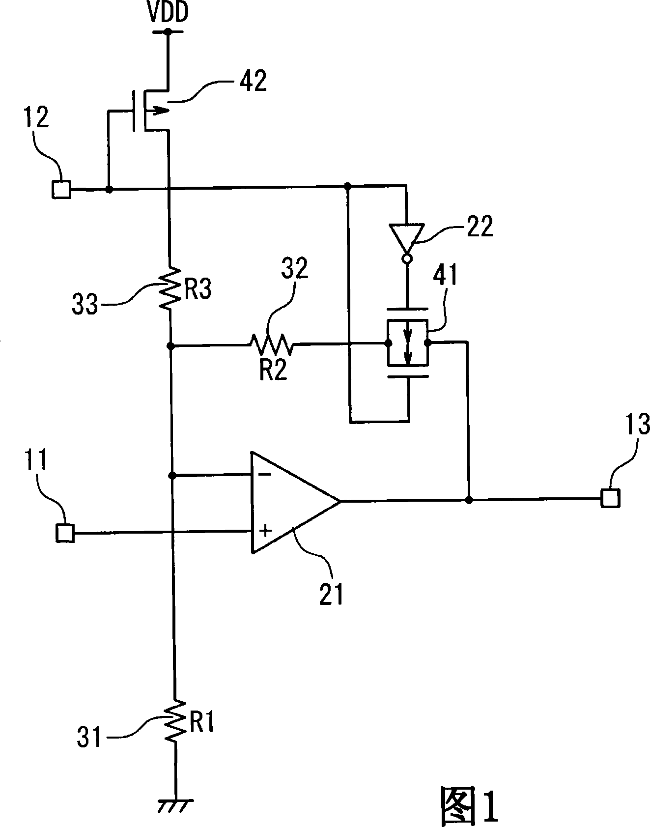
[0014] FIG. 1 is a circuit diagram illustrating the configuration of an input interface circuit according to a first embodiment of the present invention. The input interface circuit is provided with a differential amplifier 21 , an inverter circuit 22 , resistors 31 , 32 , 33 , and MOS (Metal Oxide Semiconductor) switches 41 and 42 . The MOS switch 41 is composed of a transmission gate including PMOS and NMOS transistors having a source and drain connected in common, and the MOS switch 42 is composed of a PMOS transistor. In the following, the resistances of the resistors 31, 32, 33 are referred to as R1, R2 and R3, respectively. The signal input 11 is connected to the non-inverting input of a differential amplifier 21 (indicated by the sign "+"). The MOS switch 42 and the resistors 33 and 31 are connected in series between the first power supply line VDD of the power supply level Vdd and the second power supply line GND of the ground level. The control terminal of the MOS s...
no. 2 example
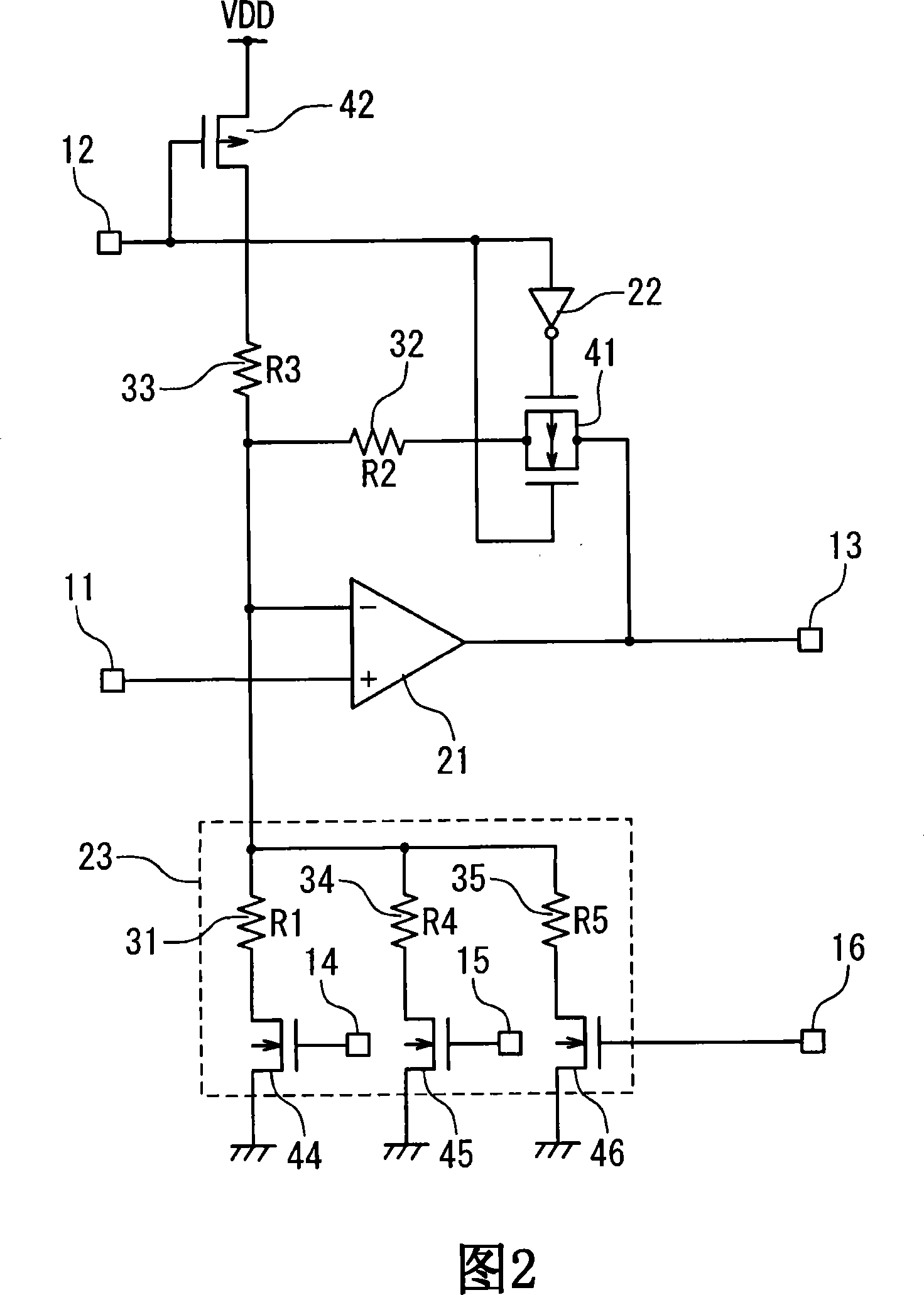
[0030] FIG. 2 is a circuit diagram illustrating the structure of an input interface circuit according to a second embodiment of the present invention. The input interface circuit according to the second embodiment is provided with a differential amplifier 21 , an inverter circuit 22 , resistors 32 and 33 , MOS switches 41 and 42 , and a synthesized resistor circuit 23 . It should be noted. The structure of FIG. 2 is almost the same as that of FIG. 1 except that the resistor 31 in FIG. 1 is replaced by a composite resistor circuit 23 . The resultant resistor circuit 23 includes resistors 31 , 34 , 35 and MOS switches 44 to 46 . In this embodiment, NMOS transistors are used as the MOS switches 44 to 46 .
[0031] The signal input 11 is connected to the non-inverting input of a differential amplifier 21 (indicated by the sign "+"). The MOS switch 42, the resistor 33, and the combined resistor circuit 23 are connected in series between the power supply line VDD and the ground l...
no. 3 example
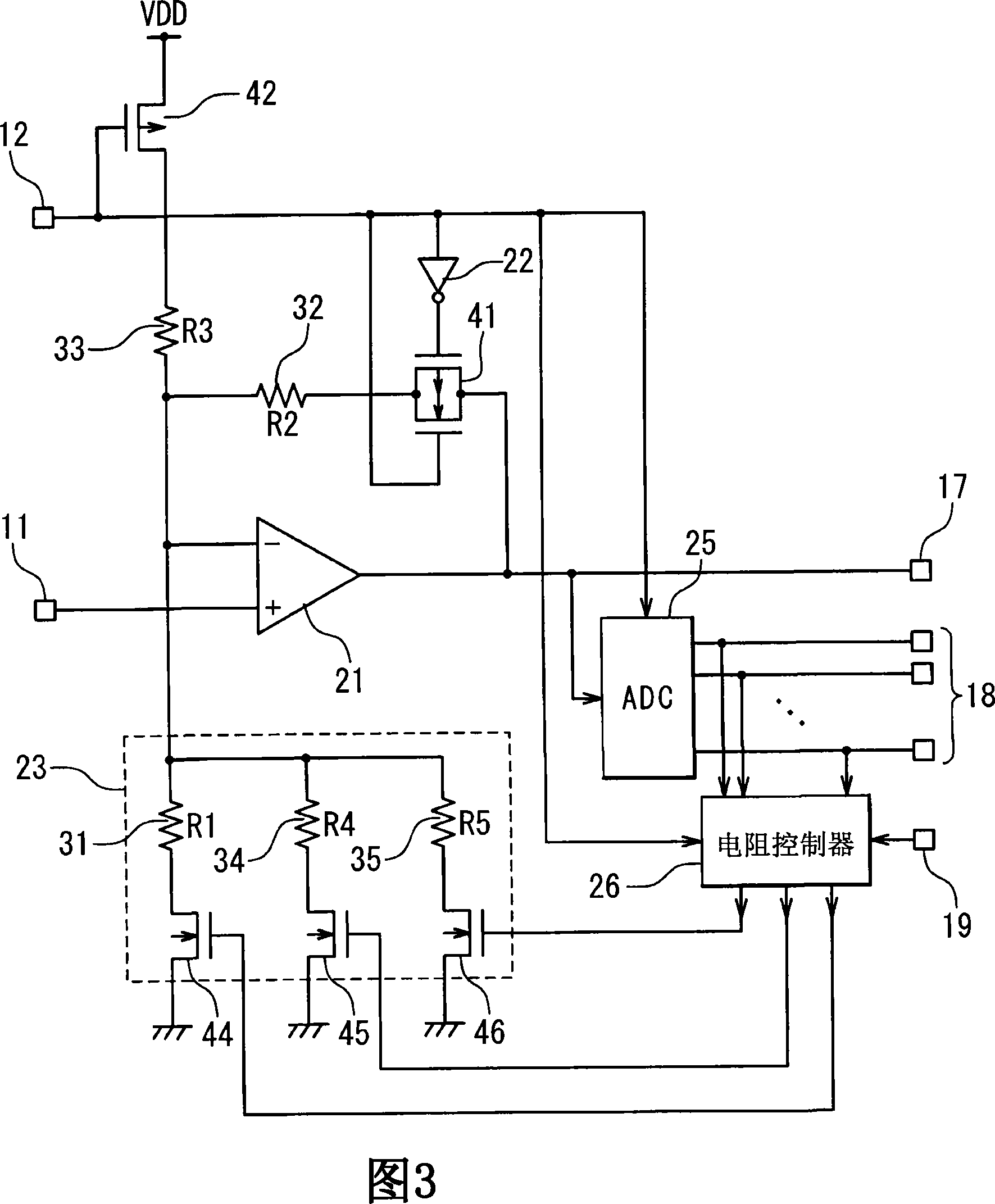
[0053] FIG. 3 is a circuit diagram illustrating the structure of an input interface circuit according to a third embodiment of the present invention. The input interface circuit according to the third embodiment is configured to provide, in addition to gain-variable analog amplification, A / D conversion of an analog input signal to generate a corresponding digital signal. Semiconductor ICs are often required to process analog input signals after converting them into digital signals, and the structure of the input interface circuit according to the third embodiment meets this need.
[0054] The input interface circuit according to the third embodiment is provided with a differential amplifier 21, an inverter circuit 22, resistors 32 and 33, MOS switches 41 and 42, a synthesis resistor circuit 23, an A / D converter 25, and a resistance controller 26 . The composite resistor circuit 23 includes resistors 31 , 34 and 35 and MOS switches 44 to 46 . The structure of the input interf...
PUM
 Abstract
Description
Claims
Application Information
 - R&D
- Intellectual Property
- Life Sciences
- Materials
- Tech Scout
- Unparalleled Data Quality
- Higher Quality Content
- 60% Fewer Hallucinations
Browse by: Latest US Patents, China's latest patents, Technical Efficacy Thesaurus, Application Domain, Technology Topic, Popular Technical Reports.
© 2025 PatSnap. All rights reserved.Legal|Privacy policy|Modern Slavery Act Transparency Statement|Sitemap|About US| Contact US: help@patsnap.com