A test shell circuit and its design method

A technology for testing enclosures and design methods, applied in the directions of monitoring/monitoring/test arrangement, electrical components, transmission monitoring, etc., can solve problems such as the influence of the total test time of the chip, mismatches, etc., to reduce the number of transmitted data packets and optimize the design. , improve the effect of parallelism

Active Publication Date: 2008-01-09
INST OF COMPUTING TECH CHINESE ACAD OF SCI
View PDF0 Cites 11 Cited by
  • Summary
  • Abstract
  • Description
  • Claims
  • Application Information

AI Technical Summary

Problems solved by technology

The network channel structure is designed and configured according to the operation of the network on chip in the working mode, so there may be a mismatch between the network channel bandwidth of a core logic and the number of core scan chains under test
This problem will not affect the test time of a single core, but the waste of network channels will bring additional network traffic, so it will have a huge impact on the total test time of the entire chip

Method used


Image

  • A test shell circuit and its design method
  • A test shell circuit and its design method
  • A test shell circuit and its design method

Examples


Embodiment

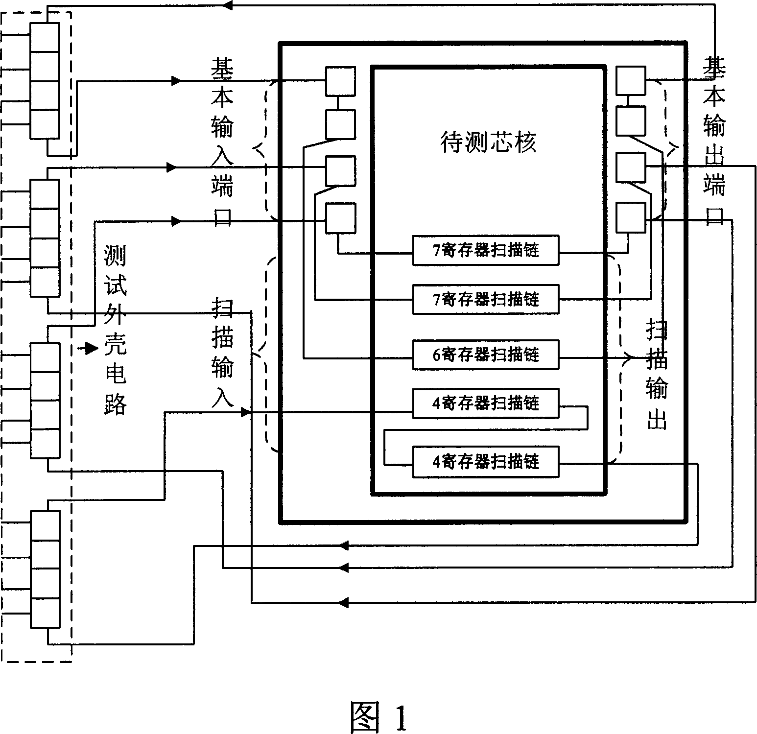
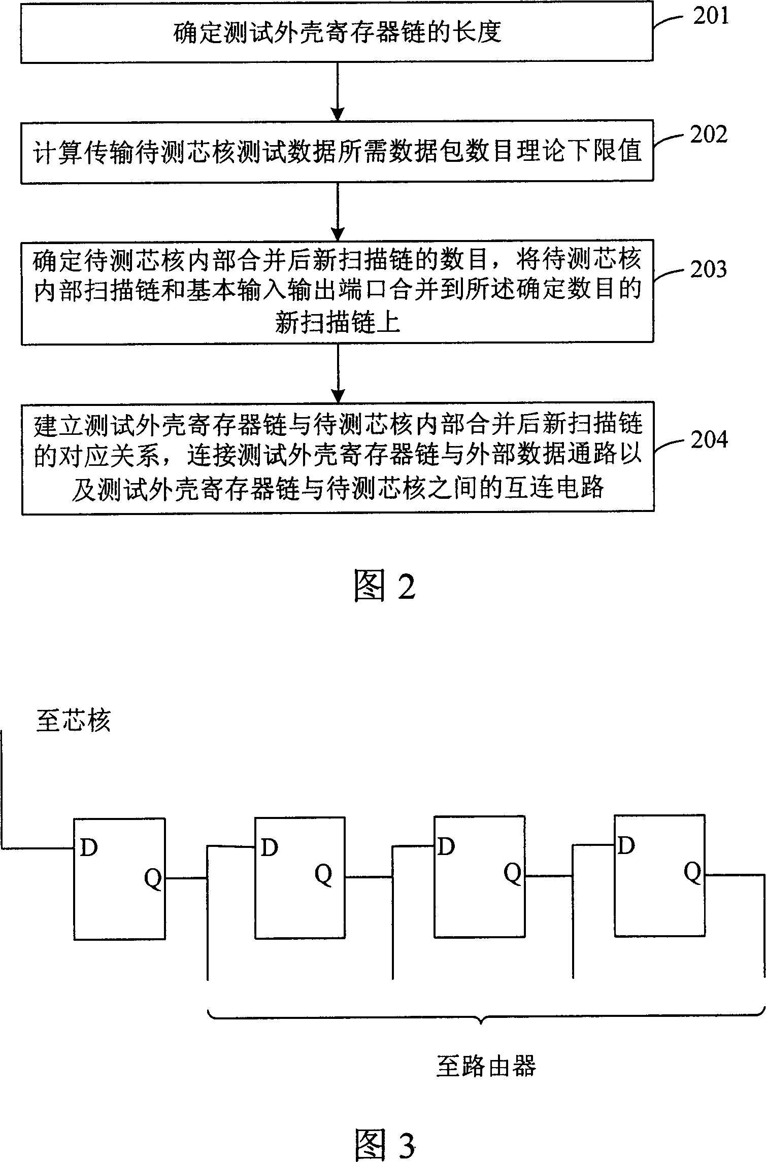
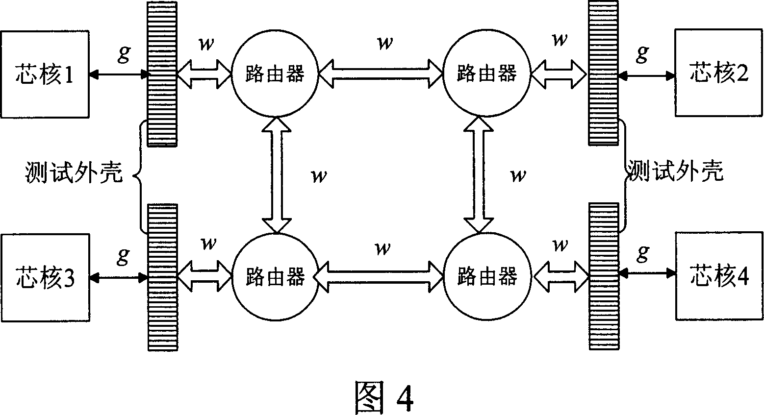
[0073] In this embodiment, it is assumed that a core to be tested contains 15 scan chains containing 45 registers, 5 scan chains containing 20 registers, and 108 input / output ports, 108 being the number of input ports and output ports The maximum value between the numbers, the bandwidth w of the data path is 16, then according to the total number N of the test shell registers is equal to the bandwidth w of the data path, it can first be determined that the total number N of the test shell registers is 16.

[0074] Then, calculate the theoretical lower limit of the number of data packets required to transmit the core test data to be tested according to formula (1):

[0075]

[0076] Then, since w=16, try to allocate the test shell registers to g groups in the order of {16, 8, 4, 2, 1}.

[0077] First, assuming g=16, the number of registers l on each new scan chain including the added basic input and output ports shall not exceed (N / g)×n p =(16 / 16)×56=56. On the premise tha...


PUM


Abstract

The invention comprises: at least one test enclosure register chain used for testing the core to be tested; an interconnection circuit for connecting said test enclosure register chain to the core to be tested; an interconnection circuit for connecting said test enclosure register chain to the external data channel. The invention also reveals a method for designing the test enclosure circuit.

Description

technical field [0001] The invention relates to the technical field of testability design of integrated circuit chips, in particular to a test shell circuit designed for the bandwidth of an on-chip network data path and a design method thereof. Background technique [0002] Future SoCs will integrate hundreds or thousands of cores on a single chip made up of billions of transistors. Such a system-on-a-chip will require communication components with bandwidths of tens of gigabits per second, which must be reusable in order to meet time-to-market requirements. Many research works have proposed the use of switching networks as an alternative to interconnecting SoC cores. Such a network, known as a network-on-chip (NoC), addresses two key requirements for future systems: reusability and variable bandwidth. Many recent studies have shown that the network-on-chip will become the optimal solution for on-chip interconnection of system cores in the future. [0003] If the network ...

Claims


Application Information

Patent Timeline
Patent Type & Authority Applications(China)
IPC IPC(8): H04L12/26H04B17/00H04M3/24H04B17/30
Inventor 李佳胡瑜李晓维
Owner INST OF COMPUTING TECH CHINESE ACAD OF SCI
Why Eureka
Try Eureka