
Multilayer printed circuit board

A multi-layer printing and circuit board technology, which is applied in the manufacture of multi-layer printed circuit boards and the field of multi-layer printed circuit boards, can solve the problems that the mask and the laser device cannot match the position of the substrate, and the electrical connection cannot be obtained. , to achieve the effect of improving the conductivity and adhesion

Inactive Publication Date: 2008-01-09
IBIDEN CO LTD
View PDF0 Cites 7 Cited by
  • Summary
  • Abstract
  • Description
  • Claims
  • Application Information

AI Technical Summary

Problems solved by technology

[0032] However, since the positioning marks formed on the IC chip are completely hidden by applying the metal film over the entire surface, the mask drawn with wiring, etc., and the laser device, etc. cannot be aligned with the position of the substrate.
Therefore, the positions of the pads of the IC chip and the through holes are deviated, and electrical connection cannot be obtained.

Method used


Image

  • Multilayer printed circuit board
  • Multilayer printed circuit board
  • Multilayer printed circuit board

Examples


Embodiment 1

[0104] First, the configuration of the multilayer printed wiring board according to the first embodiment of the present invention will be described with reference to the cross section of the multilayer printed wiring board 10 shown in FIG. 6 .

[0105] The multilayer printed circuit board shown in FIG. 6 is composed of a core substrate 30 accommodating an IC chip 20 , an interlayer resin insulating layer 50 , and an interlayer resin insulating layer 150 . The through hole 60 and the conductive circuit 58 are formed on the interlaminar resin insulating layer 50 , and the through hole 160 and the conductor circuit 158 ​​are formed on the interlaminar resin insulating layer 150 .

[0106] The IC chip 20 is covered with a passivation film 24 , and a die pad 24 constituting an output terminal is arranged in an opening of the passivation film 24 . Over the die pad 24 made of aluminum, a transition layer 38 is formed. The transition layer 38 is composed of three layers of the first ...

Embodiment 2

[0208] Next, the structure of the multilayer printed wiring board according to the second embodiment of the present invention will be described with reference to the cross section of the multilayer printed wiring board shown in FIG. 18 .

[0209] The multilayer printed circuit board 210 shown in FIG. 18 is composed of a core substrate 230 accommodating an IC chip 220 , an interlayer resin insulating layer 250 , and an interlayer resin insulating layer 350 . The through hole 260 and the conductive circuit 258 are formed on the interlayer resin insulating layer 250 , and the through hole 360 ​​and the conductive circuit 358 are formed on the interlayer resin insulating layer 350 .

[0210] A passivation film 224 is covered on the IC chip 220 , and a die pad 224 constituting an output terminal and a positioning mark 223 are arranged in an opening of the passivation film 224 . On top of the pad 224, a transition layer 238 consisting mainly of copper is formed.

[0211] On the int...

Embodiment 3

[0243] Next, the structure of the multilayer printed wiring board according to the third embodiment of the present invention will be described with reference to the cross section of the multilayer printed wiring board 410 shown in FIG. 26 .

[0244] The multilayer printed circuit board 410 shown in FIG. 26 is composed of a core substrate 430 accommodating an IC chip 420 , an interlayer resin insulating layer 450 , and an interlayer resin insulating layer 550 . The through hole 460 and the conductive circuit 458 are formed on the interlayer resin insulating layer 450 , and the through hole 560 and the conductive circuit 558 are formed on the interlayer resin insulating layer 550 .

[0245] An IC protective film (passivation+polyimide) 422 is overlaid on the IC chip 420 , and an aluminum die pad 424 constituting an output terminal is arranged in an opening of the IC protective film 422 . On the surface of the die pad 424, an oxide coating film 426 is formed. On the die pad 424,...


PUM


Abstract

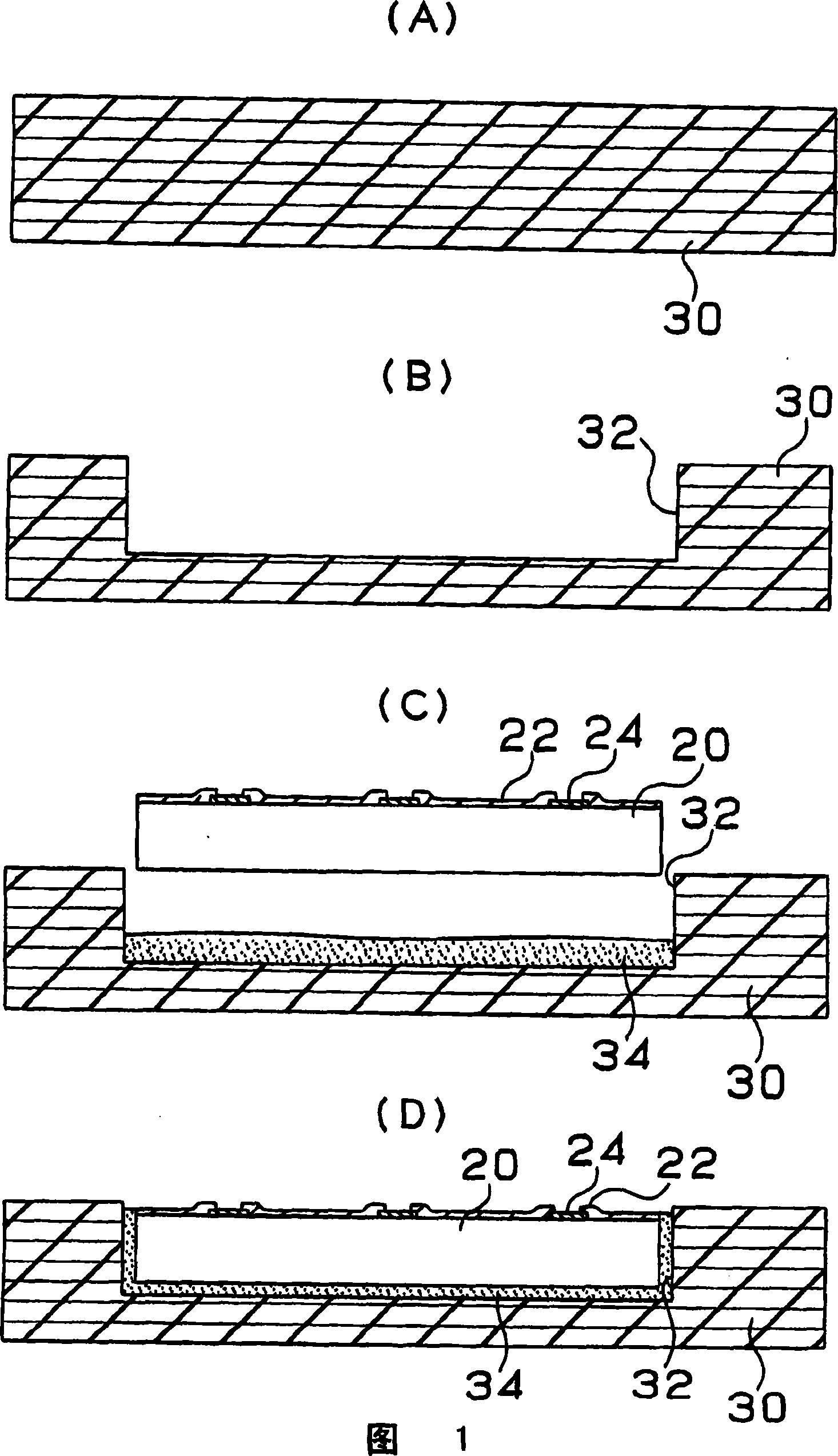
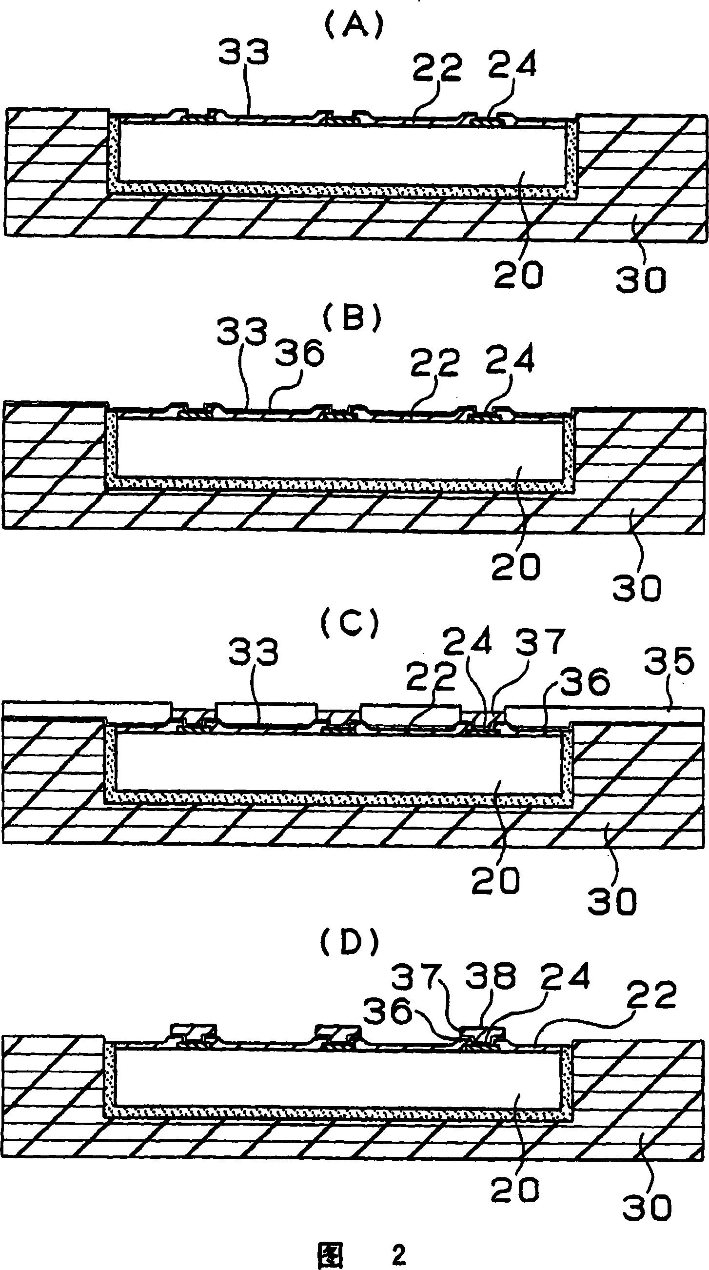
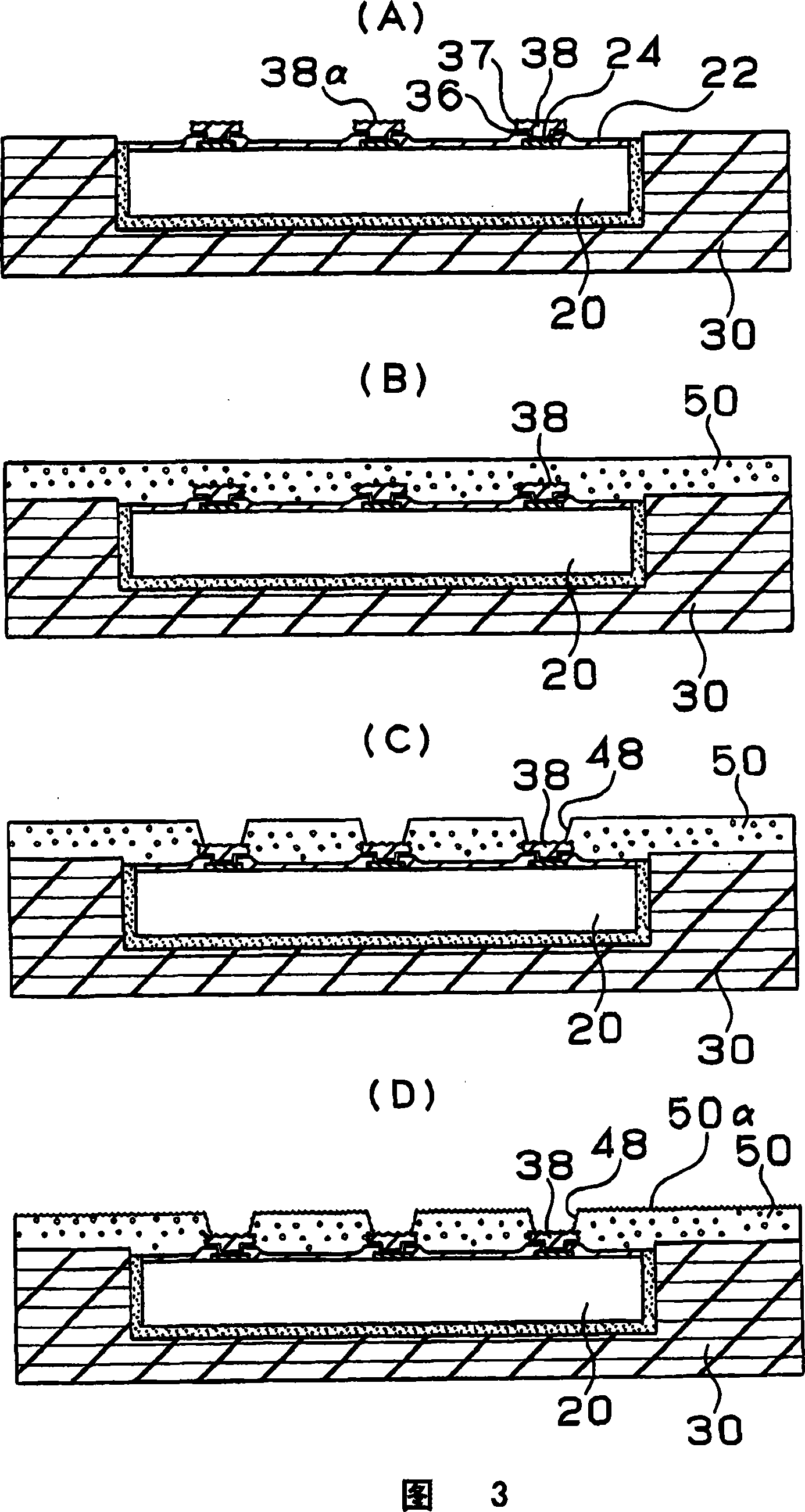
A multilayer printed circuit board has an IC chip 20 included in a core substrate 30 in advance and a transition layer 38 provided on a pad 24 of the IC chip 20 . Due to this, it is possible to electronically connect the IC chip to the multilayer printed circuit board without using lead members and a sealing resin. Also, by providing the transition layer 38 made of copper on the die pad 24 , it is possible to prevent resin residues on the pad 24 and to improve connection characteristics between the pad 24 and a via hole 60 and reliability.

Description

[0001] This application is a divisional application of: [0002] Title of invention: Multilayer printed circuit board and method for manufacturing multilayer printed circuit board [0003] International filing date: January 12, 2001 [0004] Application number: 01805638.5 technical field [0005] The present invention relates to a build-up multilayer printed circuit board, in particular to a multilayer printed circuit board incorporating electronic components such as IC chips and a method for manufacturing the multilayer printed circuit board. Background technique [0006] The IC chip is electrically connected to the printed circuit board by a mounting method such as wire bonding, TAB, or flip-chip bonding. [0007] Wire connection is to mold the IC chip to the printed circuit board with an adhesive, connect the pads of the printed circuit board and the pads of the IC chip with wires such as metal, and then apply thermosetting resin to protect the IC chip and the wires. O...

Claims


Application Information

Patent Timeline
Patent Type & Authority Applications(China)
IPC IPC(8): H05K1/18H05K1/02H01L23/544H01L21/60H01L23/13H01L23/498H01L23/538
CPCH01L2924/01015H01L2924/01023H01L2224/24227H01L2924/01046H01L2924/15153H01L2924/01082H01L2223/54486H01L2924/01018H01L2924/01025H01L2924/01002H01L2924/1517H01L2924/01019H01L2924/15311H01L24/19H01L2223/5448H01L2924/01029H01L2924/01027H01L2223/54473H01L2924/15312H01L2924/01013H01L2924/30107H01L2924/01024H01L2924/0103H01L2224/92H01L2224/20H01L2924/01047H01L2924/01079H01L24/24H01L2224/92244H01L2224/04105H01L2924/14H01L2924/01005H01L2924/01033H01L2924/01006H01L2223/54426H01L2924/0102H01L2924/01078H01L2924/01011H01L2924/01012H01L2224/19H01L2224/24H01L2224/32225H01L2224/73267H01L2224/83H01L2224/82H01L2924/00012
Inventor 坂本一杉山直王东冬苅谷隆
Owner IBIDEN CO LTD
Learn More