Chemical and mechanical grinding method

A grinding method and chemical mechanical technology, which is applied in the direction of surface polishing machine tools, grinding/polishing equipment, electrical components, etc., can solve the problems of needing to replace the grinding fluid, lack of versatility, and inconvenient implementation, and achieve low cost , Eliminate surface scratches and increase the difficulty of the process

Active Publication Date: 2008-01-16
SEMICON MFG INT (SHANGHAI) CORP +1
View PDF1 Cites 14 Cited by
  • Summary
  • Abstract
  • Description
  • Claims
  • Application Information

AI Technical Summary

Problems solved by technology

However, on the one hand, this method is too targeted and only applicable to tungsten metal, not applicable to other grinding thin layers, and is not universal; on the other hand, it needs to replace the grinding liquid, which is not convenient to implement and the cost is also high

Method used


Image

  • Chemical and mechanical grinding method
  • Chemical and mechanical grinding method
  • Chemical and mechanical grinding method

Examples


Embodiment Construction

[0054] In order to make the above objects, features and advantages of the present invention more comprehensible, specific implementations of the present invention will be described in detail below in conjunction with the accompanying drawings.

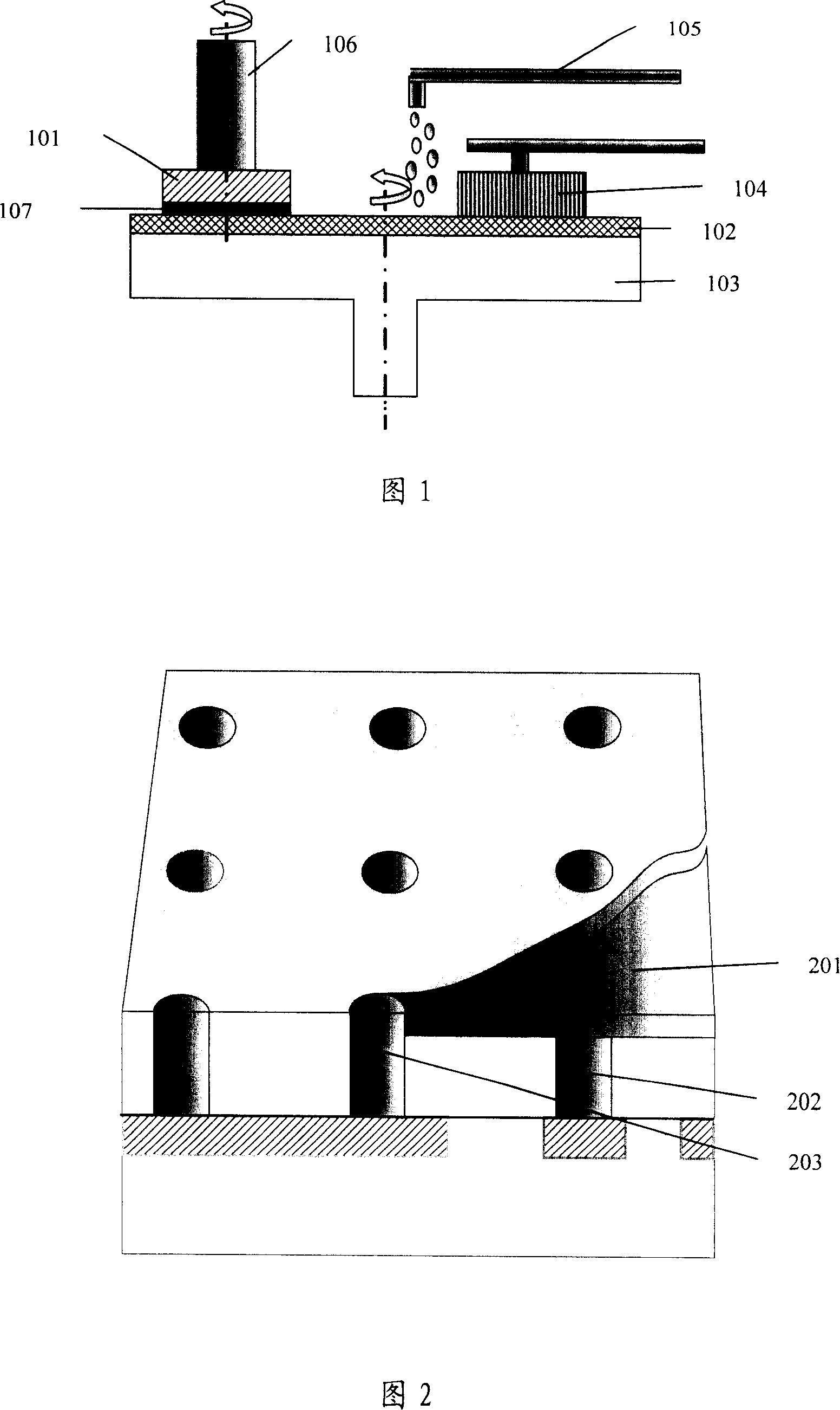
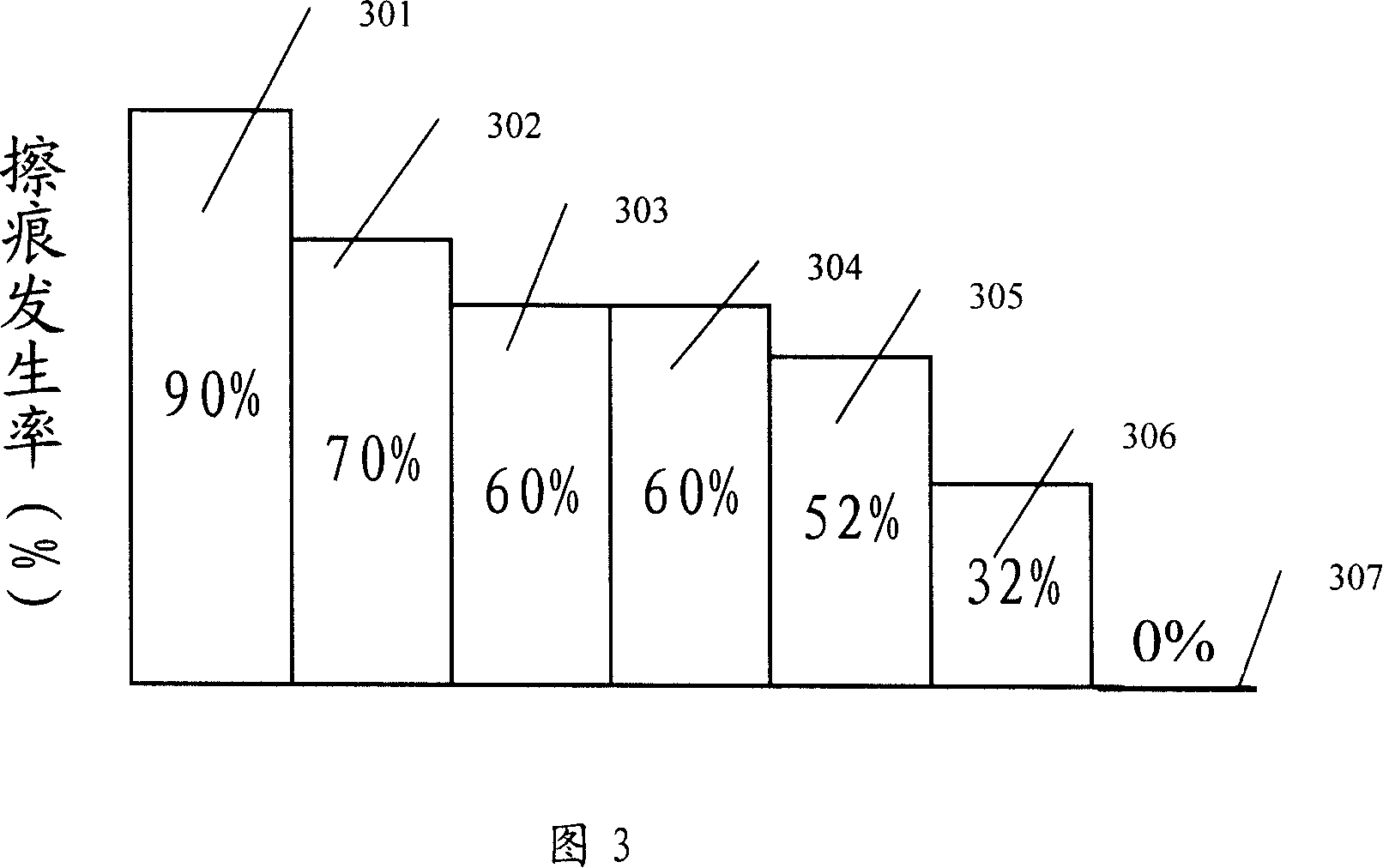
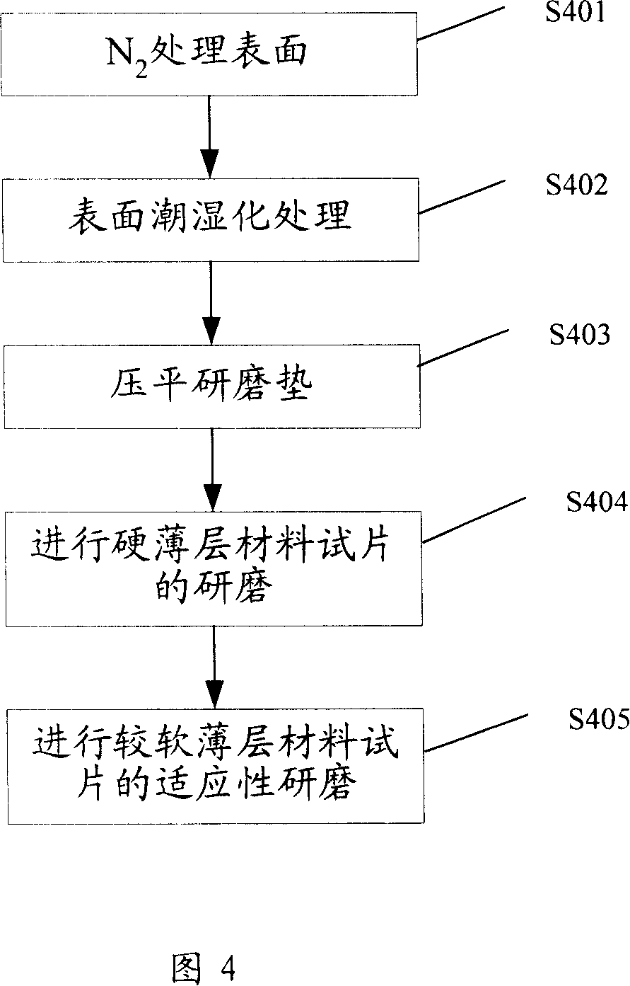
[0055] Chemical mechanical polishing (CMP) technology has been widely used in the field of integrated circuit manufacturing because of its excellent global planarization performance. However, it is found that it tends to form some tiny scratches on the surface of the wafer during the manufacturing process, which may cause an electrical short circuit of the wafer. The chemical mechanical polishing method of the present invention, based on the characteristics of the CMP process, combined with a large number of experimental data, can significantly reduce or even eliminate surface scratches through the improvement of the CMP process conditions, and improve the process quality without increasing the difficulty of the process.

[0056] Gener...


PUM


Abstract

The invention discloses a chemical mechanical grinding method, which reduces or even eliminates scratches produced easily in the chemical mechanical grinding process by processing a grinding pad and improving grinding process. The invention is applicable in various CMP thin materials with characteristics of universality and low cost. On the premise that process difficulty is not increased, the invention improves the rate of the finished products.

Description

technical field [0001] The invention relates to the field of semiconductor manufacturing, in particular to a chemical mechanical grinding method. Background technique [0002] With the rapid development of ULSI (Ultra Large Scale Integration), the manufacturing process of integrated circuits has become more and more complex and sophisticated. In order to improve integration and reduce manufacturing costs, the feature size of components (Feature Size) continues to decrease, and the number of components per unit area of ​​the chip continues to increase. It is difficult for planar wiring to meet the requirements of high-density distribution of components, and only multi-layer wiring technology can be used. The vertical space of the chip is utilized to further increase the integration density of the device. However, the application of multi-layer wiring technology will cause the surface of the silicon wafer to be uneven, which is extremely unfavorable for graphics production. ...

Claims


Application Information

Patent Timeline
Patent Type & Authority Applications(China)
IPC IPC(8): B24B29/00H01L21/304
Inventor 俞昌杨春晓臧伟
Owner SEMICON MFG INT (SHANGHAI) CORP
Why Eureka
Try Eureka