

Semiconductor device and its manufacturing method
A manufacturing method and semiconductor technology, applied in the direction of semiconductor devices, semiconductor/solid-state device components, electric solid-state devices, etc., can solve the problems of thickening of the thickness of the semiconductor device, increase of the thickness of the semiconductor device, increase of the cost, etc., and the manufacturing process will not be Complicated effect
- Summary
- Abstract
- Description
- Claims
- Application Information
AI Technical Summary
Problems solved by technology
Method used
Image

Examples
Embodiment approach 1
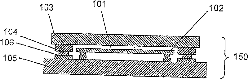
[0092] figure 1 It is a sectional view of the semiconductor device showing the basic structure of the semiconductor device of the present invention.
[0093] As shown in the figure, the semiconductor device 150 is three-dimensionally mounted with two semiconductor chips 101 and 103 by flip-chip mounting.
[0094] That is, on the first semiconductor chip (lower semiconductor chip) 101, a bump electrode (a low-level electrode: hereinafter referred to as a first electrode) 102 formed by metal plating or the like is formed, and the first electrode 102 It is directly connected to a predetermined wiring pattern 106 formed on the substrate 105 . That is, the first semiconductor device is mounted on the main surface of the substrate 105 by flip-chip mounting.
[0095] Similarly, a tall electrode 104 (hereinafter referred to as a second electrode) is formed on the second semiconductor chip 103 , and the second electrode 104 is directly connected to a predetermined wiring pattern 106 ...
Embodiment approach 2
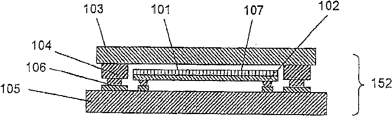
[0120] Figure 4 It is a cross-sectional view of a semiconductor device showing another example of the semiconductor device of the present invention (an example in which a first semiconductor chip and a second semiconductor chip are integrated). exist Figure 4 In , the same reference signs are attached to the parts common to the above-mentioned illustrations, and the description of the common parts will be omitted. This also applies to the illustrations below.
[0121] In the aforementioned embodiments, the two semiconductor chips are flip-chip mounted separately, but in this embodiment, the two semiconductor chips (101, 103) are first bonded, and then flip-chip mounted. The integrated semiconductor chips are mounted on the substrate 105 together.
[0122] That is, in the above-mentioned embodiments, the first semiconductor chip 101 and the second semiconductor chip 103 are not in contact or in a state of not being closely attached, but in this embodiment, the upper surfac...
Embodiment approach 3
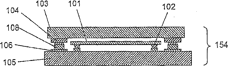
[0134] Figure 5 It is a cross-sectional view of a semiconductor device showing another example of the semiconductor device of the present invention (an example in which the entire semiconductor device is sealed with resin).
[0135] In the present embodiment, the package structure is formed by sealing the bare chips (101, 103) with resin, thereby improving the water resistance or environment resistance of the semiconductor device. Such as Figure 5 As shown, the semiconductor device 158 of this embodiment is provided with a resin sealing body 109 for sealing the entire semiconductor device (other structures are the same as figure 1 same).
[0136] The sealing resin 109 is composed of epoxy resin, polyimide resin, acrylic resin, silicone resin, etc. with high heat resistance (glass transition temperature: 120-180°C), and preferably does not contain corrosion-inducing components such as halogen and organic phosphoric acid. . In addition, the curing temperature of the sealin...
PUM
 Abstract
Description
Claims
Application Information