High voltage MOS transistor circuit simulated macro model

A technology of MOS transistors and simulation models, which is applied in the direction of electrical digital data processing, special data processing applications, instruments, etc., can solve problems such as lack of physical meaning, complex extraction process, and high difficulty, so as to achieve convenient and fast extraction of parameters and model simulation Accurate and portable results

Active Publication Date: 2008-01-23
SHANGHAI INTEGRATED CIRCUIT RES & DEV CENT
View PDF0 Cites 11 Cited by
  • Summary
  • Abstract
  • Description
  • Claims
  • Application Information

AI Technical Summary

Problems solved by technology

As shown in Figure 2, a high-voltage transistor macro model currently used in the industry is mainly composed of a variable resistor connected in series to the drain D' and source S' of an ordinary SPICE transistor. However, the high-voltage transistor macro model The model has the following limitations, which prevent it from being widely used in the industry:
[0007] 1. Use a variable resistor whose resistance value changes with the terminal voltage to simulate the lightly doped drain diffusion region of the high-voltage MOS transistor, which only meets the simulation needs in terms of mathematical empirical formulas, and does not have physical meaning,

Method used


Image

  • High voltage MOS transistor circuit simulated macro model
  • High voltage MOS transistor circuit simulated macro model
  • High voltage MOS transistor circuit simulated macro model

Examples


Embodiment Construction

[0030] The high-voltage MOS transistor circuit simulation macro model of the present invention will be further described in detail below.

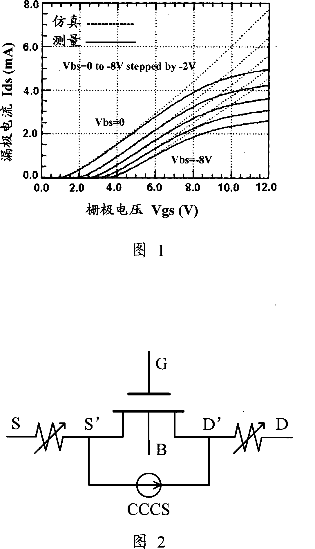
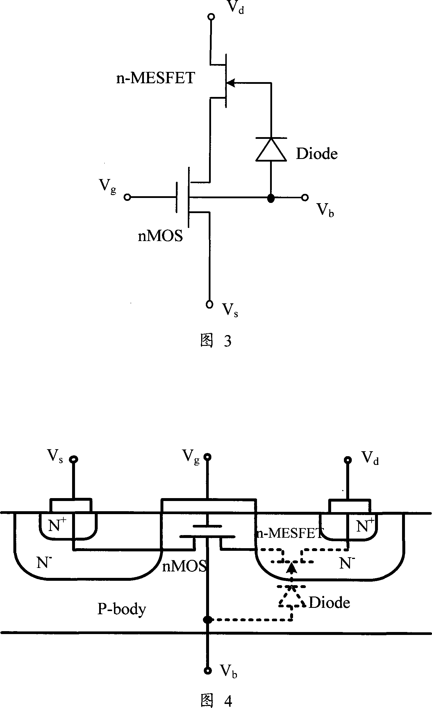
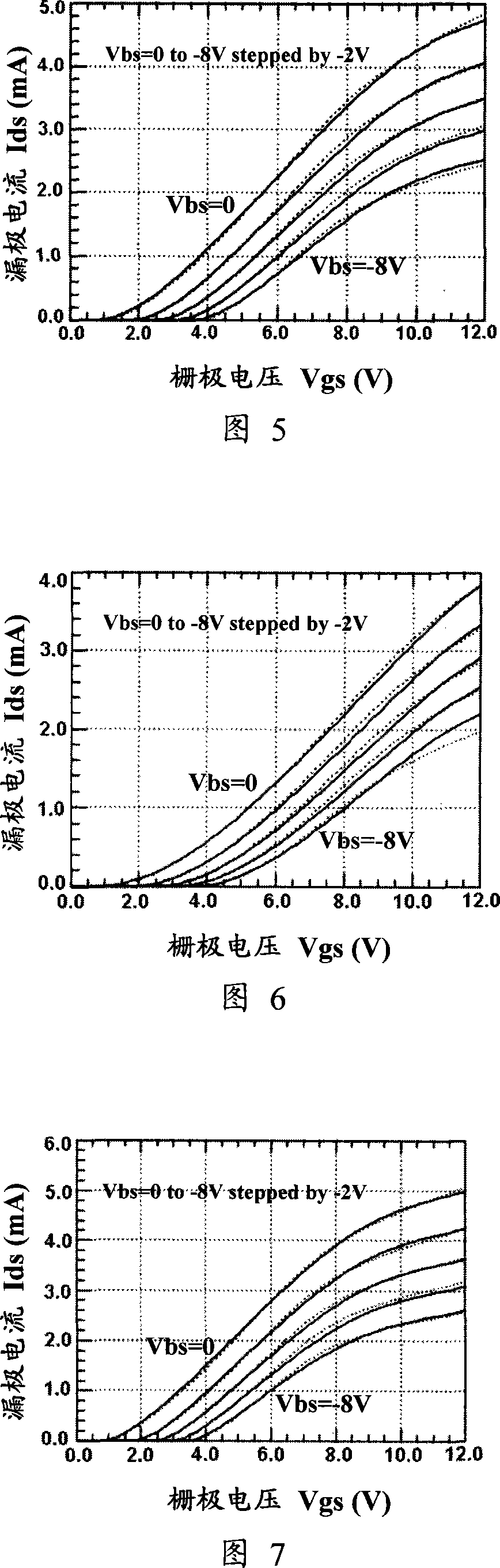
[0031] As shown in Figure 3, the high-voltage MOS transistor circuit emulation macro model of the present invention comprises a MOS transistor emulation model nMOS, an n-channel JFET emulation model n-MESFET and a diode emulation model Diode, and its specific circuit connection mode is: in nMOS The n-MESFET is connected in series on the drain of the nMOS, and the Diode is connected in series between the drain and the gate of the nMOS. The variable resistance characteristic of JFET is used to simulate the lightly doped drain diffusion region of the high-voltage MOS transistor, and the diode is used to simulate the equivalent PN junction between the substrate and the N-type drain.

[0032] Figure 4 is a schematic diagram of the structure of a high-voltage MOS transistor. The position of each circuit component (nMOS, n-MESFET, Diode) of the s...


PUM


Abstract

The invention provides a high-voltage MOS transistor circuit simulation macro model, which belongs to the technical field of integrated circuit. The invention comprises a MOS transistor simulation model, an n channel JFET simulation model and a diode simulation model. The n channel JFET is connected in series in a drain electrode of the MOS transistor; the diode is connected in series between a source electrode and grid electrode of the MOS transistor. The invention has clear physic significance and its features can vary along the changes in parameter. Therefore, the invention can be supported and applied in all ordinary circuit simulator, EDA software and model software of the industry. Besides, the invention has the advantages of convenient and express extraction as well as accurate and fast simulation.

Description

technical field [0001] The invention belongs to the field of integrated circuits, in particular to a circuit simulation macro model of a high-voltage MOS transistor. Background technique [0002] In recent years, high-voltage MOS transistors have been widely used in circuits such as circuit output interfaces, LCD drivers, and power management chips. While improving the withstand voltage of the device, the cost is greatly reduced. The wide application of high-voltage MOS transistors makes more and more very large-scale integration (VLSI) designs and simulations require accurate high-voltage MOS transistor models. [0003] The structure of the high-voltage MOSFET is significantly different from that of the standard process low-voltage MOS transistor (LV MOSFET): the well depth, gate oxide thickness (Tox) and channel length of the high-voltage MOS transistor are larger than those of the low-voltage MOS transistor, most notably the high-voltage MOS transistor A lightly doped r...

Claims


Application Information

Patent Timeline
IPC IPC(8): G06F17/50
Inventor 任铮胡少坚
Owner SHANGHAI INTEGRATED CIRCUIT RES & DEV CENT
Why Eureka
Try Eureka