High efficiency light emitting diode with surface mini column array structure using diffraction effect

A technology of light-emitting diodes and micro-pillar arrays, which is applied in the manufacture of semiconductor devices, electrical components, and semiconductor/solid-state devices, etc., to achieve the effect of high utilization of light-emitting area, improved utilization of surface light-emitting area, and simple production.

Inactive Publication Date: 2008-01-23
SHENZHEN UNIV +1
View PDF2 Cites 16 Cited by
  • Summary
  • Abstract
  • Description
  • Claims
  • Application Information

AI Technical Summary

Problems solved by technology

However, since the light emitted by general LEDs is incoherent light, whether the micro-rods are arranged periodically does not affect the light extraction efficiency

Method used


Image

  • High efficiency light emitting diode with surface mini column array structure using diffraction effect
  • High efficiency light emitting diode with surface mini column array structure using diffraction effect
  • High efficiency light emitting diode with surface mini column array structure using diffraction effect

Examples


Embodiment Construction

[0028] The present invention will be further described below in conjunction with the accompanying drawings.

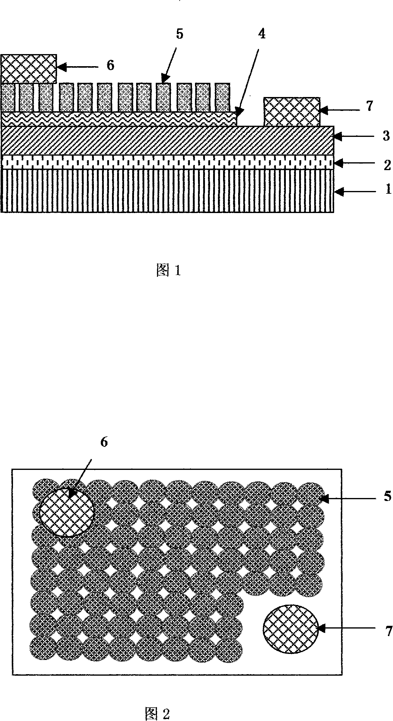
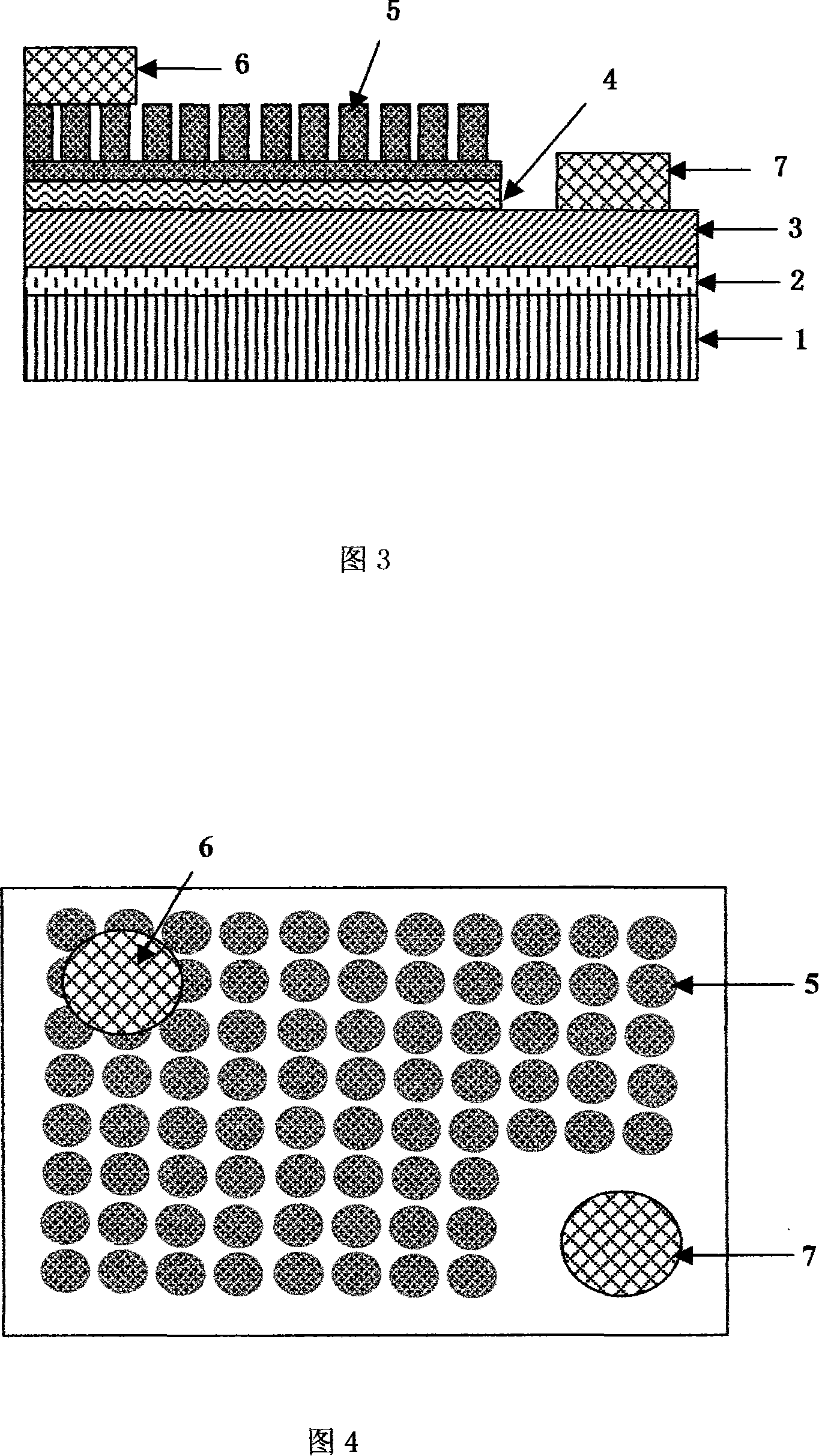
[0029] 1. Referring to FIG. 1, a GaN buffer layer is first deposited on a sapphire substrate, and then an LED epitaxial wafer is grown thereon.

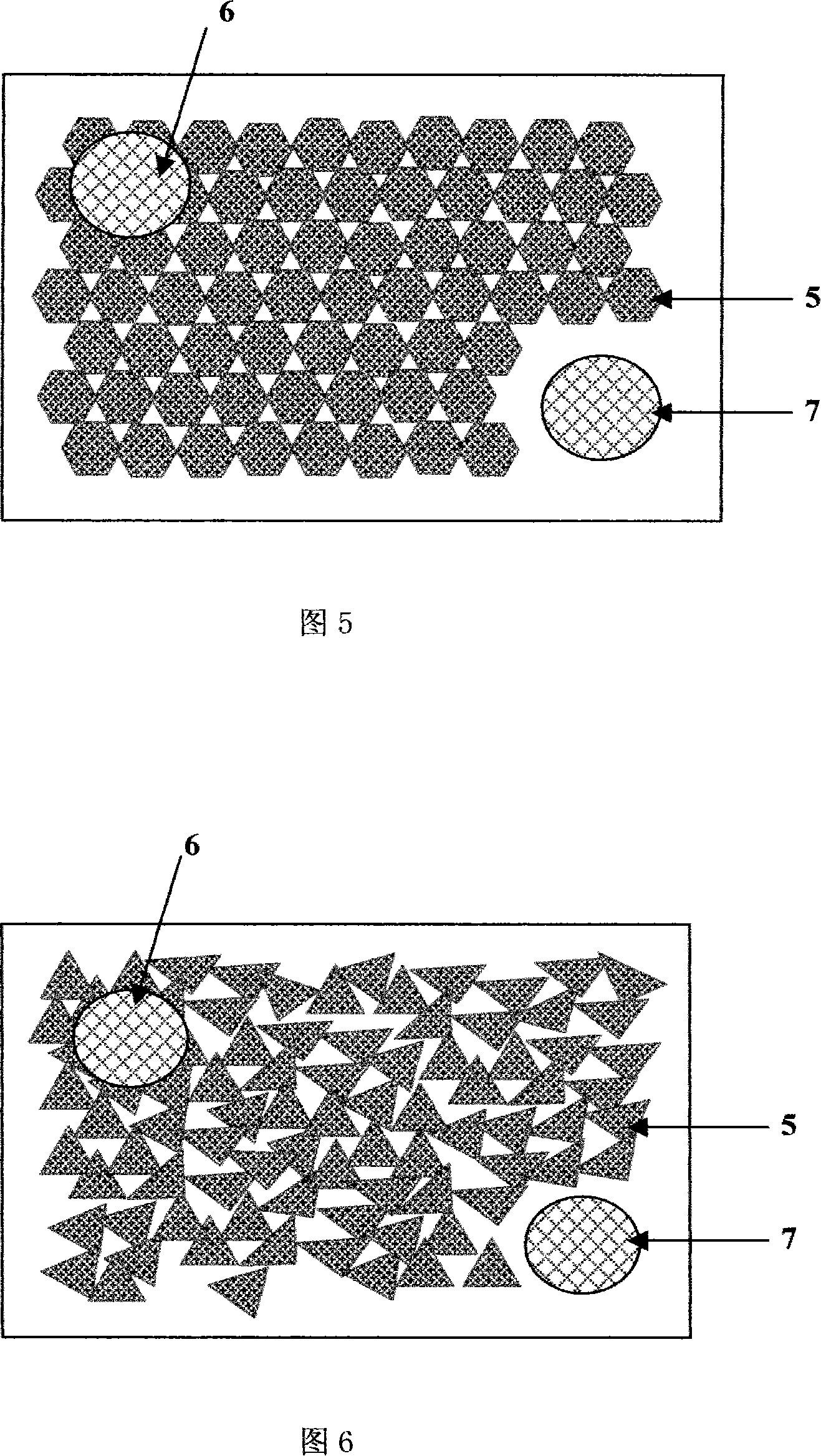
[0030] 2. The micro-pillar array is etched on the P-type GaN layer by using the mask method, photolithography and dry etching technology.

[0031] 3. Prepare electrodes on N-type GaN, and prepare N-type pads on the electrodes; prepare electrodes on P-type GaN mesa, and prepare P-type pads on the electrodes. The electrode to be laid can be a transparent electrode, which is laid on the entire GaN layer; a common metal electrode with a simple structure can also be used. Ordinary metal material electrodes with complex pattern shapes can also be used.


PUM


Abstract

A high-efficiency LED provided with a surface micro-column array structure and based on diffraction effect has a structure below: N type GaN grows on a cushioning layer of a sapphire substrate. A GaN active layer grows on the N type GaN layer. A P type GaN layer grows on the active layer. A micro-column array is etched on the P type GaN layer, which can be periodically or aperiodiclaly arranged two-dimensional structure. A P type electrode and a P type bonding pad are laid on the P type GaN layer. An N type electrode and an N type bonding pad are arranged on the N type GaN layer. The present invention has the advantages that light diffusion effect is utilized and light is fully exported through the micro-column to improve lighting efficiency and ensure even light distribution on a light surface. Compared with LED adopting two-dimensional photonic crystal, the structure needs simple production technique and lower production cost. Compared with traditional LED suffering roughly processed surfaces, the structure brings much higher light emission efficiency.

Description

(1) Technical field [0001] The invention relates to a high-brightness GaN-based light-emitting diode, in particular to a micro-pillar array structure that utilizes diffraction effect to improve luminous efficiency. (2) Background technology [0002] How to improve the light-emitting efficiency of light-emitting diodes is an important research direction in light-emitting diode technology. When a point light source propagates through a medium at a certain distance and exits the air, due to the total reflection effect of light at the interface, only light with an angle smaller than a certain angle can exit, which limits the light extraction efficiency of the LED. In response to this problem, people use the method of microstructure to improve the outgoing direction of the outgoing light, so as to improve the probability of light outgoing. The patent with the authorized announcement number is CN1874012A; the band gap characteristic of the two-dimensional photonic crystal is used...

Claims


Application Information

Patent Timeline
Patent Type & Authority Applications(China)
IPC IPC(8): H01L33/00H01L51/50H01L51/52H01L33/10H01L33/20H01L33/22
CPCH01L33/22H01L33/20H01L33/10
Inventor 欧阳征标许桂雯
Owner SHENZHEN UNIV
Why Eureka
Try Eureka