Supercharge Your Innovation With Domain-Expert AI Agents!

Light-emitting element and method for manufacturing light-emitting element

一种发光元件、制造方法的技术,应用在半导体/固态器件制造、制造工具、电气元件等方向,能够解决Au-Sn系焊料层剥离问题不容易获得解决等问题

Inactive Publication Date: 2008-01-23
SHIN-ETSU HANDOTAI CO LTD
View PDF3 Cites 10 Cited by
  • Summary
  • Abstract
  • Description
  • Claims
  • Application Information

AI Technical Summary

Problems solved by technology

[0009] However, the inventors of the present invention found that even if the structure of the above-mentioned Patent Document 3 is adopted, the problem of peeling off of the Au-Sn-based solder layer is not easily solved.

Method used


Image

  • Light-emitting element and method for manufacturing light-emitting element
  • Light-emitting element and method for manufacturing light-emitting element
  • Light-emitting element and method for manufacturing light-emitting element

Examples


Embodiment Construction

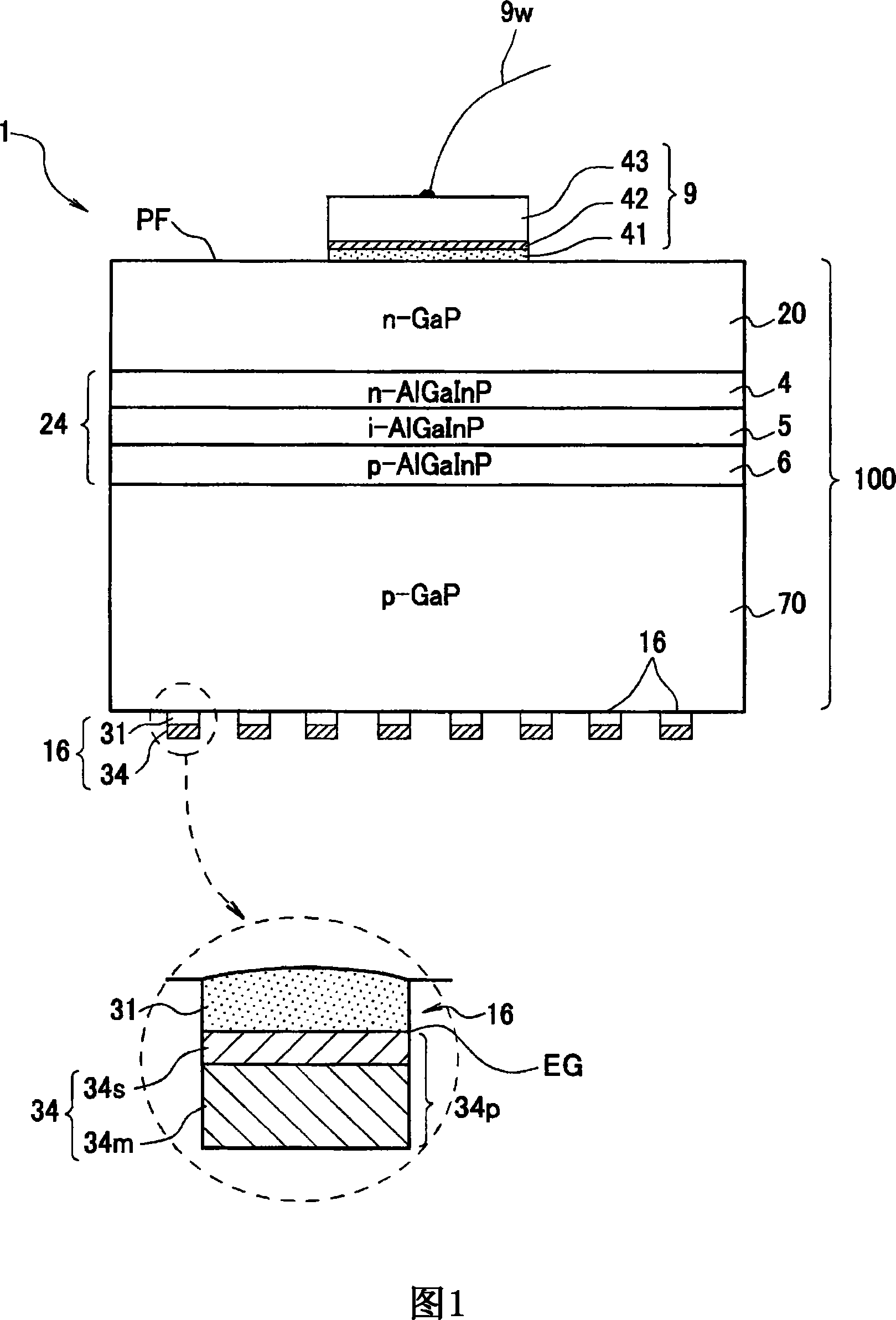
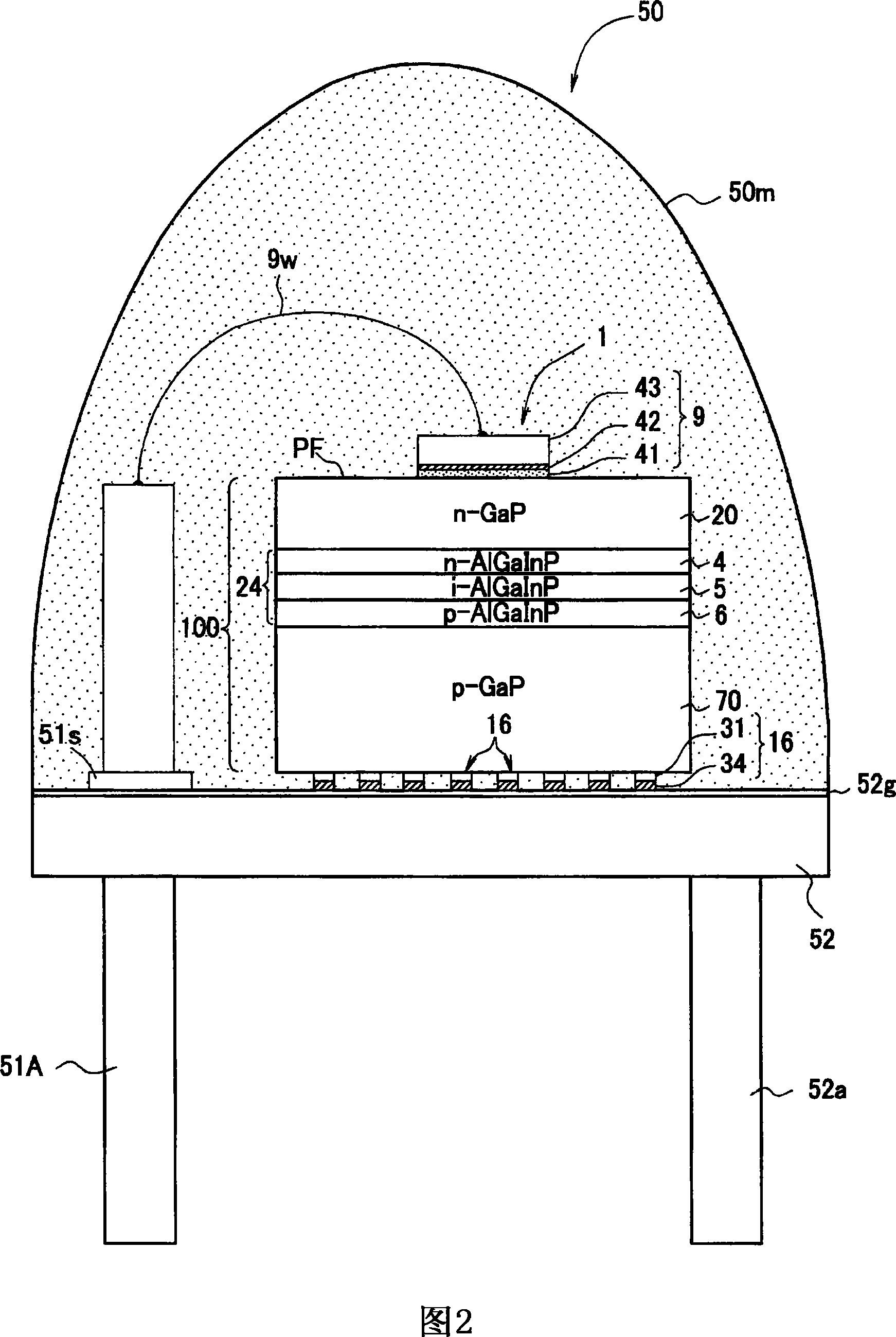
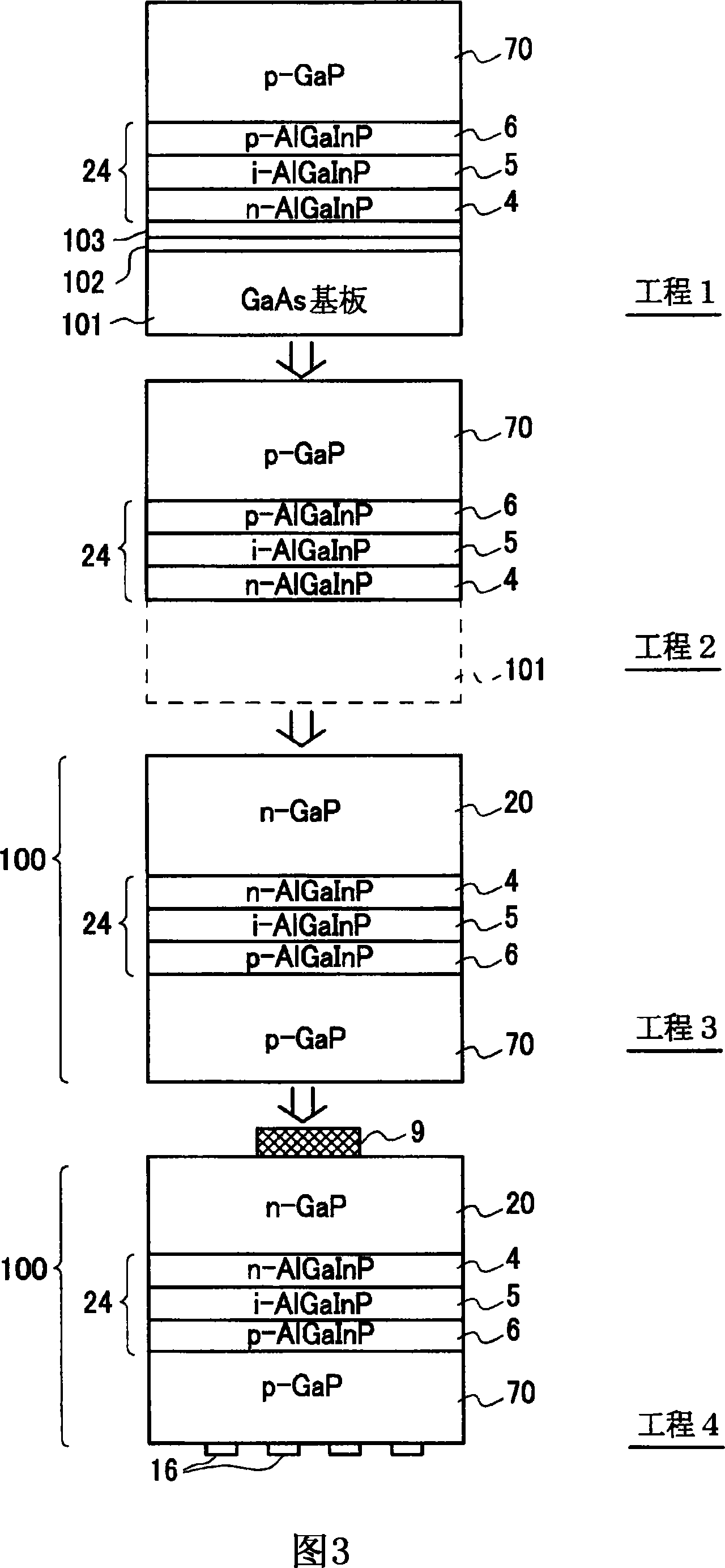
[0066] Hereinafter, embodiments of the method of manufacturing a light-emitting element according to the present invention will be described with reference to the drawings. Fig. 1 is a schematic conceptual diagram of a light-emitting element to which the present invention is applied. The light-emitting element 1 has the main surface on the light extraction surface side of the compound semiconductor layer 100 having the light-emitting layer portion 24 as the first main surface, and the main surface on the opposite side as the second main surface. The first electrode 9 and the second electrode 16 are respectively formed on the second main surface. The second electrode 16 has a bonding alloyed layer 31 and a solder layer 34, the bonding alloyed layer 31 is provided in contact with the second main surface of the compound semiconductor layer 100 to reduce the bonding resistance with the compound semiconductor layer 100, the The solder layer 34 is used to connect the bonding metal ...


PUM

PropertyMeasurementUnit
melting pointaaaaaaaaaa

Abstract

Each second electrode formed on a second main surface of a compound semiconductor layer of a light emitting device has an alloyed contact layer disposed contacting the second main surface, aimed at reducing contact resistance with the compound semiconductor layer, and a solder layer connecting the alloyed contact layer to the conductive support. The solder layer forms therein a Sn-base solder layer disposed on the alloyed contact layer side having a melting point lower than the alloyed contact layer, and a Au-Sn-base solder layer disposed contacting the Sn-base solder layer opposed to the alloyed contact layer side, containing total Au and Sn of 80% or more, and having a melting point higher than the Sn-base solder layer. This configuration can provide excellent reliability of bonding between the Au-Sn-base solder layer and the alloyed contact layer, and consequently less causative of delamination of the Au-Sn-base solder layer.

Description

technical field [0001] The present invention relates to a light emitting element and a method for manufacturing the light emitting element. Background technique [0002] Patent Document 1: Japanese Unexamined Patent Publication No. 2-260671 [0003] Patent Document 2: Japanese Unexamined Patent Publication No. 9-27498 [0004] Patent Document 3: JP-A-2003-142731 [0005] Non-Patent Document 1: "Development of High Reliability Sn-Ag-Based Lead-Free Solder", Toyota Central Research Institute R&D review Vol.35 No.2 (2000) page 39 [0006] Light-emitting elements made of compound semiconductors have long used the main surface on the light extraction side as the first main surface and the main surface on the opposite side as the second main surface, and the second main surface on the back of the component chip is coated with silver paste. The electrode on the two main surface sides is attached to the structure of the metal stage (Patent Document 1), but in order to increase th...

Claims


Application Information

Patent Timeline
Patent Type & Authority Applications(China)
IPC IPC(8): H01L33/00H01L21/28B23K35/26H01L21/52H01L33/38H01L33/30H01L33/40H01L33/56H01L33/62
CPCH01L2224/73257H01L2224/4823H01L2224/29144H01L2924/01004B23K35/001H01L2924/01322H01L33/382B23K1/0016H01L2224/48091B23K35/3013B23K35/262H01L2924/3011H01L2224/48137H01L24/48H01L2924/01079H01L2224/48463H01L33/30H01L2933/0016H01L33/0079H01L2924/01078H01L2224/45144H01L33/62H01L33/40H01L24/31B23K2201/40H01L2924/00014H01L24/45H01L2924/181B23K2101/40H01L33/0093H01L2924/0105H01L2924/3512H01L2924/00H01L2224/05599H01L2924/00012
Inventor 池田均小原正义
Owner SHIN-ETSU HANDOTAI CO LTD
Features
  • R&D
  • Intellectual Property
  • Life Sciences
  • Materials
  • Tech Scout
  • Unparalleled Data Quality
  • Higher Quality Content
  • 60% Fewer Hallucinations
Learn More