Single chip integrated CMOS imaging sensor with dual-focus microlens array

A micro-lens array, image sensor technology, applied in semiconductor/solid-state device manufacturing, electrical components, circuits, etc., can solve the problem of quantum efficiency, light concentration efficiency and poor reliability, moisture resistance, high temperature resistance and radiation resistance, deformation, deformation Aging and other issues to achieve the effect of improving light collection and quantum efficiency, low cost, and high reliability

Inactive Publication Date: 2008-01-30
SEMICON MFG INT (SHANGHAI) CORP +1
View PDF0 Cites 8 Cited by
  • Summary
  • Abstract
  • Description
  • Claims
  • Application Information

AI Technical Summary

Problems solved by technology

But it can only form a single-focus microlens, and because of its low melting point, it has poor resistance to humidity, high temperature and radiation in high-altitude and space applications, and is easy to deform and age, so its quantum efficiency, light-gathering efficiency and reliability are poor.

Method used


Image

  • Single chip integrated CMOS imaging sensor with dual-focus microlens array
  • Single chip integrated CMOS imaging sensor with dual-focus microlens array
  • Single chip integrated CMOS imaging sensor with dual-focus microlens array

Examples


Embodiment Construction

[0057] The present invention will be described in detail below in conjunction with the accompanying drawings.

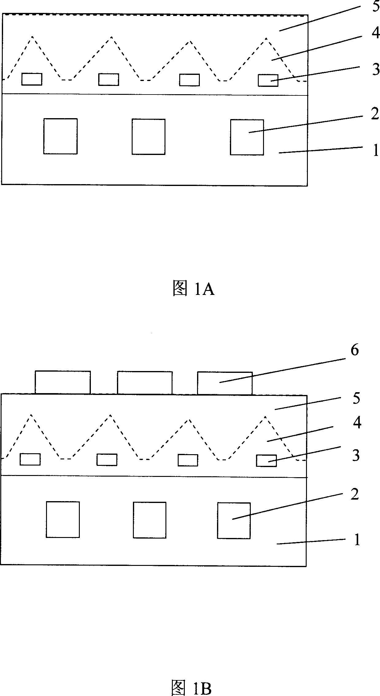
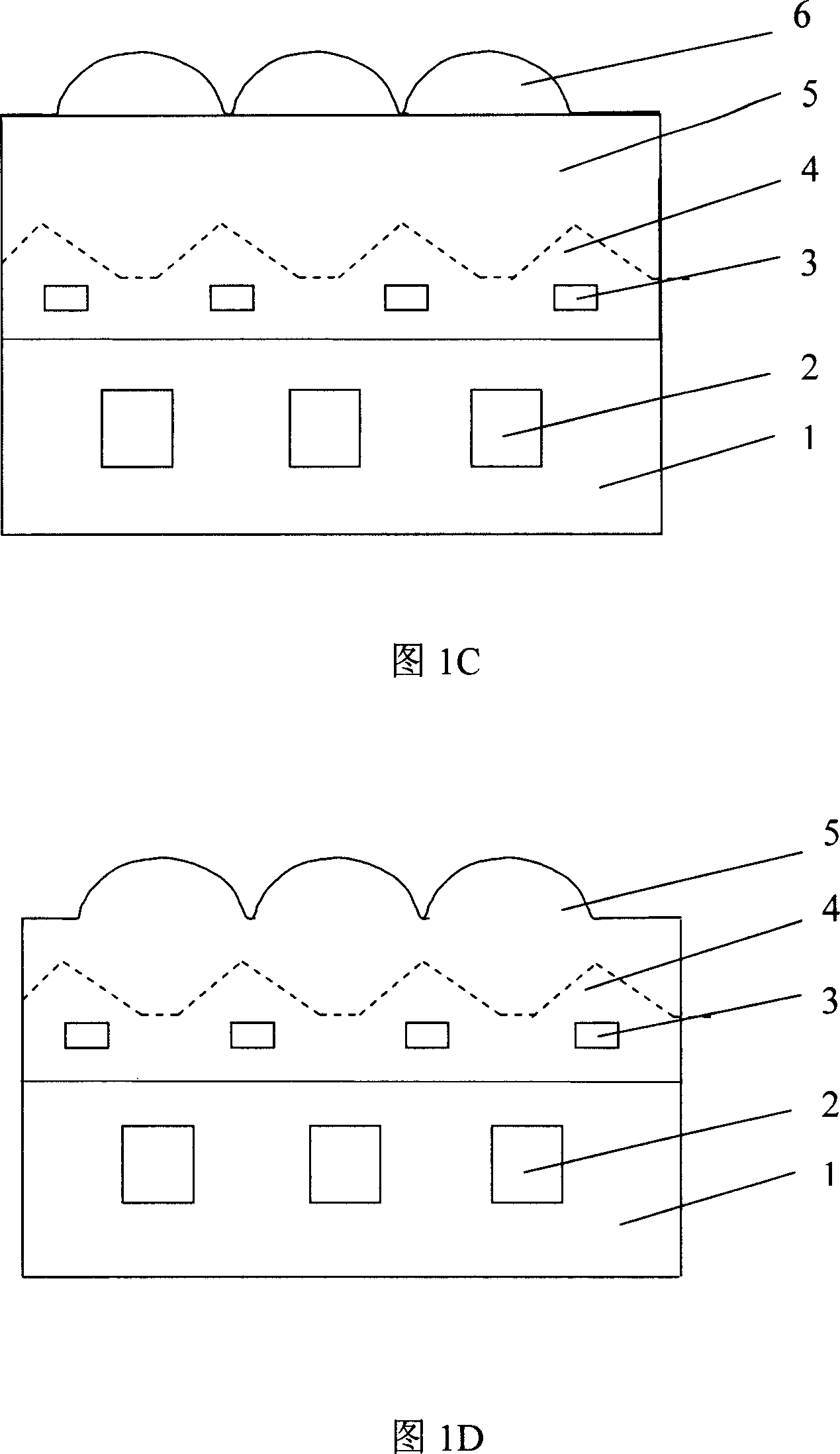
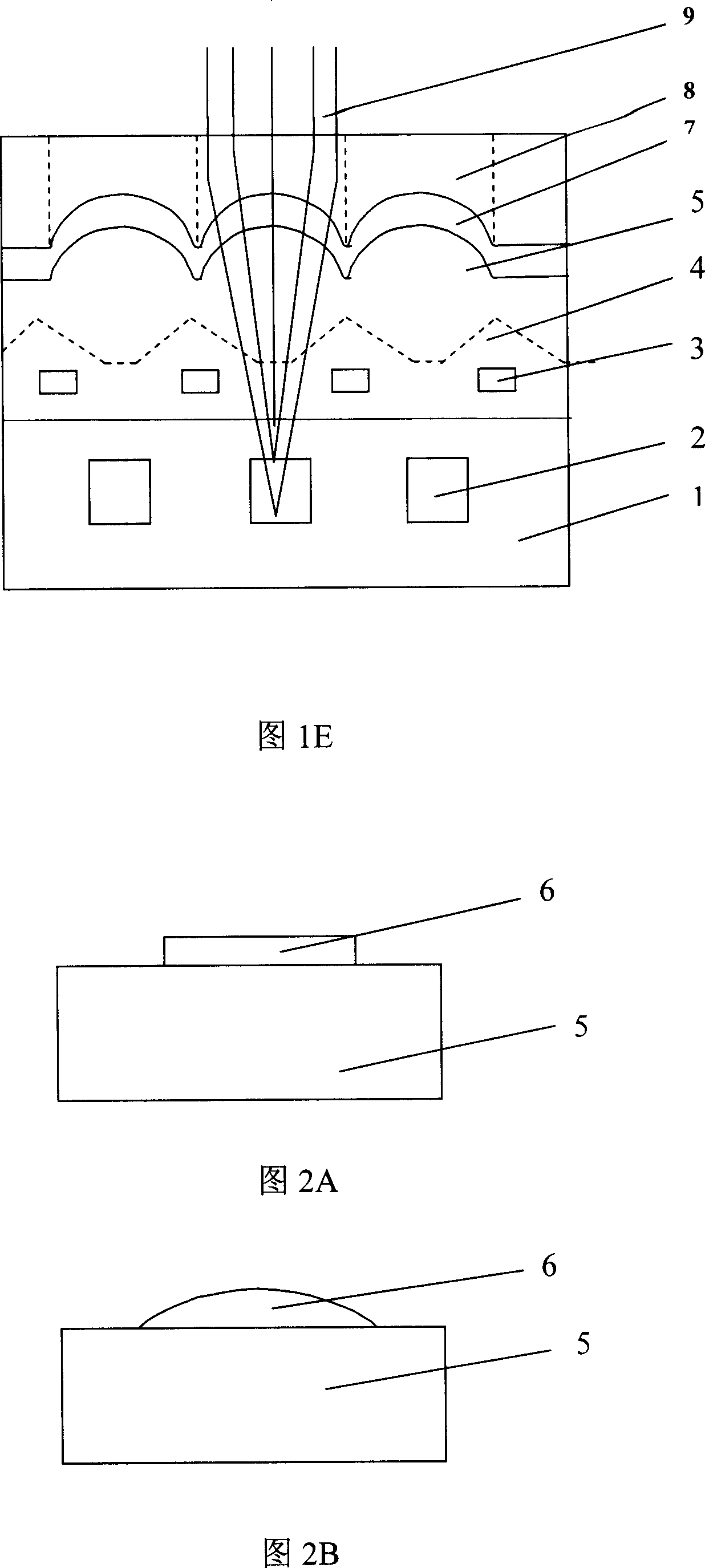
[0058] 1A-1E illustrate a monolithic integrated CMOS image sensor with a bifocal lens array and a schematic diagram of its manufacturing process according to the present invention.

[0059] According to a specific embodiment of the present invention, a monolithically integrated CMOS image sensor with a bifocal microlens array, as shown in Figure 1E, includes:

[0060] A standard CMOS logic circuit, which integrates a pin photodiode 2, has a top layer metal 3, and a silicon oxide insulating layer 4;

[0061] The microlens array 5 is integrated in the active area of ​​the CMOS circuit, more specifically, the light-absorbing surface corresponding to the pixel unit;

[0062] A silicon nitride layer 7 covering the microlens array 5;

[0063] The color filter 8 is arranged on the silicon nitride layer 7;

[0064] Among them, the bifocal microlens array is monolithically...


PUM


Abstract

A monolithically integrated CMOS image sensor with double focal micro-lens array comprises a standard CMOS logic circuit integrating a photodiode of silicon pin, a micro-lens array integrated on an optical absorption surface corresponding to an active region of the CMOS circuit, a silicon nitride layer covering the micro-lens array, a color filter arranged on the silicon nitride layer. The invention is characterized in that the micro-lens array, which is a double focal micro-lens array, is monolithically integrated with the CMOS circuit, and with a 1.44-2.0 refractive index, the micro-lens array is applied on a good optical focusing double focal micro-lens array to improve light collection efficiency and quantum efficiency.

Description

technical field [0001] The invention relates to a lens array and a manufacturing method thereof, in particular to a monolithic integrated bifocal lens array, a manufacturing method thereof and an application in a complementary metal oxide semiconductor (Complementary Metal Oxide Semiconductor, CMOS) image sensor. Background technique [0002] In the past ten years, compared with charge coupled devices (CCDs), CMOS image sensors can work at lower voltages, reduce energy consumption in portable applications, have fewer supporting circuits, and be simpler in design and provide ultra-low energy Consumption and chip-integrated image sensors have received more and more attention. These sensors, manufactured in the past by CMOS technology (0.35μm and above), generally have larger pixels than CCDs, lower resolution and lower performance. Recent technology and design developments in several areas including silicon process (0.18 μm and below), color filter array and microlens integra...

Claims


Application Information

Patent Timeline
Patent Type & Authority Applications(China)
IPC IPC(8): H01L27/146H01L21/82
Inventor 肖德元朱虹洪中山严祥成卢普生陈国庆杨建平李若加
Owner SEMICON MFG INT (SHANGHAI) CORP
Why Eureka
Try Eureka