
Method for cutting crisp material substrate
A technology for brittle material substrates and cutting methods, applied in glass cutting devices, welding/welding/cutting items, stone processing equipment, etc., can solve problems affecting product yield and damage to glass substrates, so as to improve product yield and guarantee The effect of cut quality
- Summary
- Abstract
- Description
- Claims
- Application Information
AI Technical Summary
Problems solved by technology
Method used
Image

Examples
Embodiment Construction
[0015] The present invention will be described in further detail below in conjunction with the accompanying drawings.
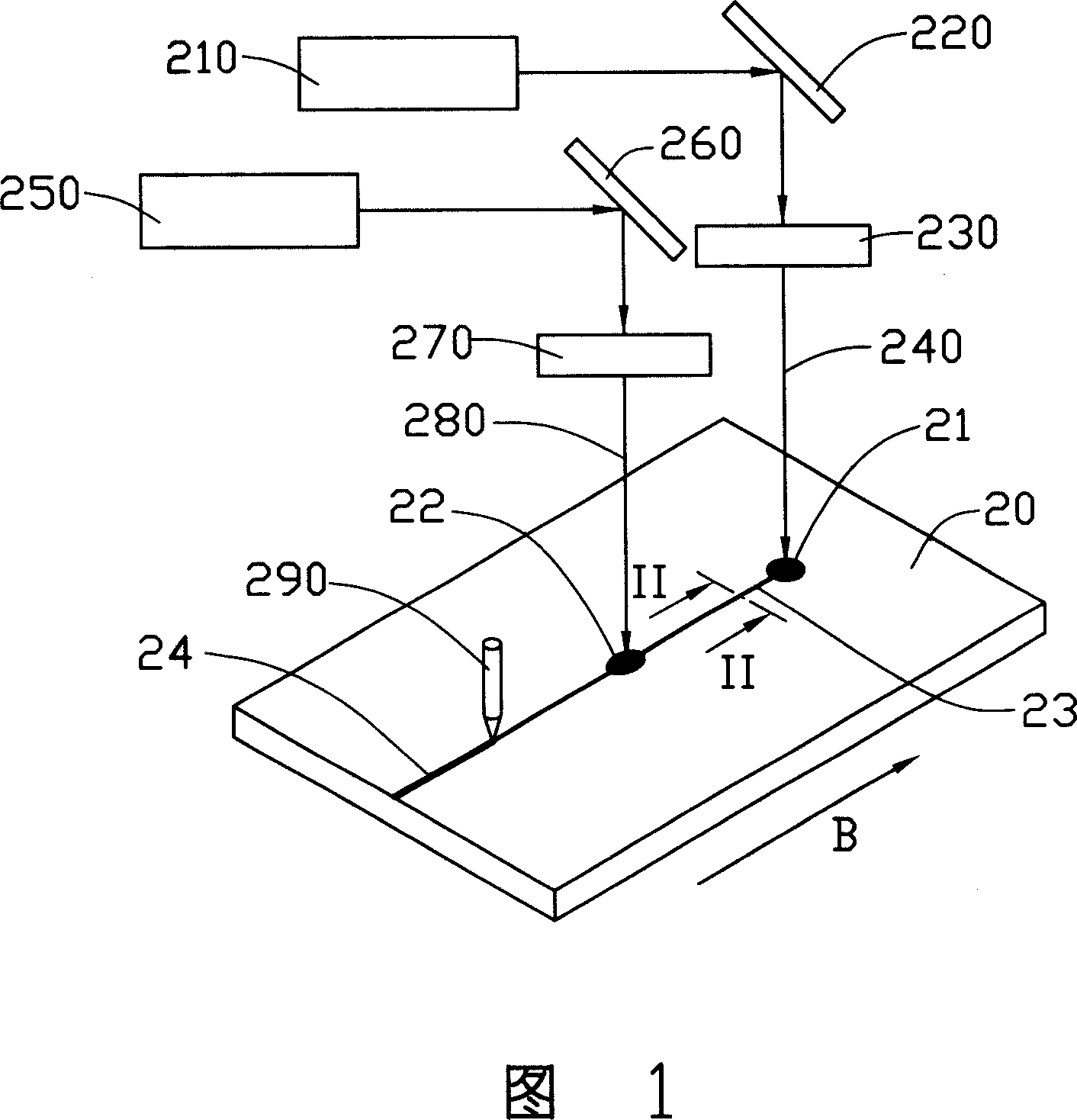
[0016] Please refer to FIG. 1, the method for cutting a brittle material substrate provided by an embodiment of the present invention includes the following steps:
[0017] (1) A brittle material substrate 20 is provided, and the brittle material substrate 20 may be a glass substrate, a ceramic substrate, a quartz substrate, a silicon wafer (Silicon Wafer) and the like.
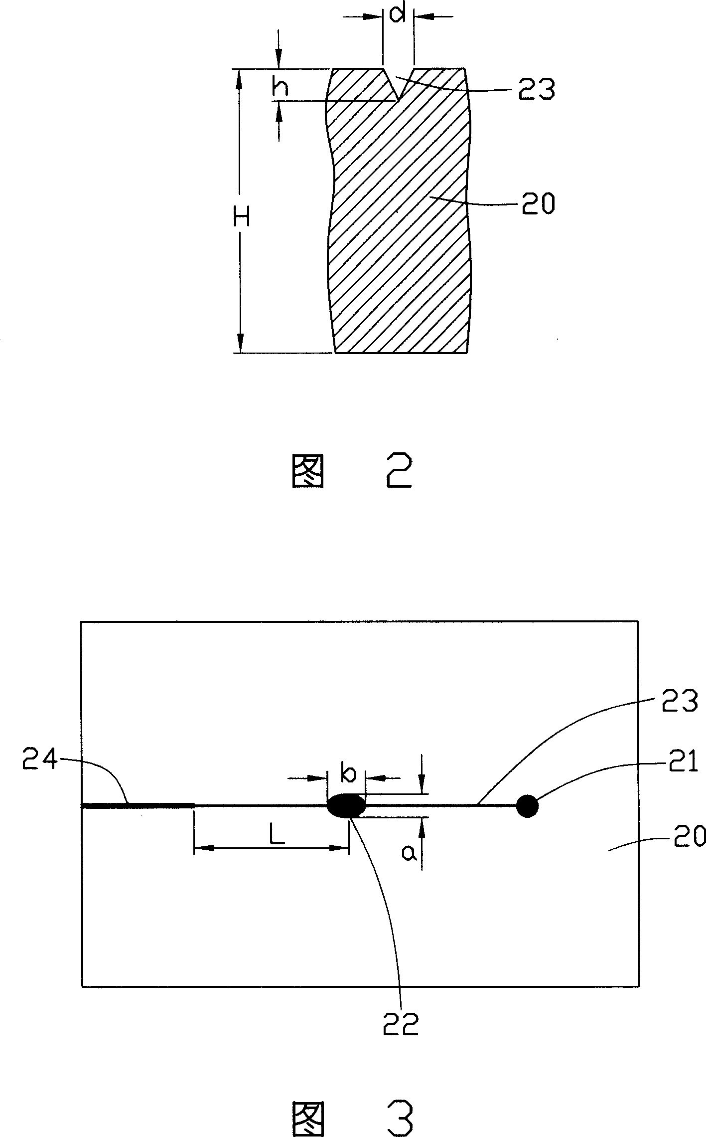
[0018] (2) Using the first laser beam 240 generated by the solid-state laser 210 to form a pre-cut line (Pre-crack) 23 on the surface of the brittle material substrate 20 . The specific steps are as follows:
[0019] The brittle material substrate 20 to be processed is placed on the carrier platform (not shown); the first laser beam 240 generated by the solid-state laser 210 is guided to the first focusing lens group 230 after passing through the first reflector 220, the first The focusing...
PUM
| Property | Measurement | Unit |
|---|---|---|
| wavelength | aaaaa | aaaaa |
| diameter | aaaaa | aaaaa |
| width | aaaaa | aaaaa |
Abstract
Description
Claims
Application Information